


 Learning with Leo: Drones—Meeting Demand Without Compromise
 Nolan’s Notes: Our Spotlight on North America
 Global Sourcing Spotlight: Building a Supply Chain That Bends, Not Breaks


Digicom Electronics to Showcase EMS Diamond Track Defect Mitigation Services at BIOMEDevice
November 30, 2016 | Digicom Electronics, Inc.Estimated reading time: 2 minutes
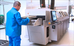
Digicom Electronics Inc., a technology and quality-driven electronics manufacturing services (EMS) company, will present its new Diamond Track Defect Mitigation Services at the BIOMEDevice Show, which will be held at the San Jose Convention Center in San Jose, California, on December 7–8, 2016. Digicom will be in Booth 327.
The program incorporates Digicom's proprietary Diamond Track nitrogen and cleaning services to reduce or eliminate defects in printed circuit boards, especially for mission critical products such as in the medical, military and aerospace, industrial, and RF wireless industries.
Digicom generates its own nitrogen to use in its solder reflow, selective soldering, and hand soldering manufacturing processes to strengthen the solder bonds and improve solder adhesion. Studies show a 50-60% reduction (as reported in TEquipment.net study) in defect levels when using nitrogen in the reflow process. Adding nitrogen minimizes device failures and ensures printed circuit board integrity.
"Adding nitrogen to the soldering process is not commonly done by EMS companies," explained Mo Ohady, general manager of Digicom Electronics. "Companies that do add it, usually do so by renting or leasing nitrogen-containing cylinders that have to be delivered in a very cold, compressed form which is not suitable for use if you're trying to maintain hot-zone stability in a reflow oven. Digicom has installed its own nitrogen generation system, producing the nitrogen and piping it through a safe, environmentally sound system so it can be used in all soldering processes – solder reflow, selective soldering, and hand soldering. Generation and on-location storage of nitrogen enable the system to have the exact amount of nitrogen it needs, eliminate temperature variability, and save money for the company, and therefore the customer."
Digicom's Diamond Track Cleaning process combines a combination of chemicals, temperature, wash cycles, timing, and equipment that results in printed circuit boards with superior quality and cleanliness. IPC-TM-650 best scenario ionic cleanliness guidelines specify an allowable level of contamination of 10-2 micrograms/in2 for military applications and 65-2 micrograms/in2 for general applications. Digicom consistently delivers better than that, with zero contamination levels, measured and verified by periodic tests done by independent labs.
Digicom helps companies with their complete process from design review through prototyping, component sourcing, manufacture, test, and process validation. Digicom is certified for ISO 9001:2008, ISO 13485:2003 medical devices quality, quality system regulation 21 CFR 820 , and ITAR certification. For more information or to arrange a meeting with Digicom at the BIOMEDevice Show or a visit at Digicom's newly expanded facility at 7799 Pardee Lane, Oakland, CA 94621, contact Digicom Electronics at +1-510-639-7003, email info@digicom.org, or see our videos, articles, and information at www.digicom.org.
Share on:


Testimonial
"We’re proud to call I-Connect007 a trusted partner. Their innovative approach and industry insight made our podcast collaboration a success by connecting us with the right audience and delivering real results."
Julia McCaffrey - NCAB GroupSuggested Items
AQUANOX A4727 and A4625 Lead KYZEN Offerings at SMTA Oregon Expo and Tech Forum
05/06/2026 | KYZENKYZEN, the global leader in innovative environmentally responsible cleaning chemistries, will exhibit at the SMTA Oregon Expo and Tech Forum scheduled to take place Thursday, May 19 at the Wingspan Event and Conference Center in Hillsboro, Oregon.
Connect the Dots: Designing for the Future of Manufacturing Reality—Surface Finish
05/07/2026 | Matt Stevenson -- Column: Connect the DotsWhen designing the complex boards that many electronic devices require to operate, designers should consider manufacturability at every step. This is my last article focused on designing for the always-evolving manufacturing reality. Choosing the right surface finish has always been important. If you are creating intricate designs with a wide variety of components, like for an ultra-high density interconnect (UHDI) board, surface finish is a critical last step.
Indium to Showcase High-Performance AI Application Solutions at SEMICON SEA 2026
05/01/2026 | Indium CorporationAs a leading provider of advanced materials solutions for today’s demanding AI applications, Indium Corporation® will feature its high-reliability product portfolio at SEMICON SEA 2026, May 5-7, in Kuala Lumpur, Malaysia.
ACCM Unveils Negative and Near-zero CTE Materials for Large-Format AI Chips
04/21/2026 | Advanced Chip and Circuit MaterialsAdvanced Chip and Circuit Materials, Inc. (ACCM) has launched two new materials: Celeritas HM50, with a negative coefficient of thermal expansion (CTE) of -8 ppm/°C to offset the positive CTE and expansion of copper with temperature on circuit boards, and Celeritas HM001, with near-zero CTE and the low-loss performance needed for high-speed signal layers to 224 Gb/s and faster in artificial intelligence (AI) circuits.
SMTA Ultra HDI Symposium, Day 2: Fragile Supply Chains, Fierce Innovation
04/14/2026 | Marcy LaRont, I-Connect007The Arizona weather yielded another beautiful day as we gathered for the second day of SMTA’s annual UHDI symposium. After the first full day discussing the role of AI in business and the how-tos of implementation, Avondale Mayor Mike Pineda kicked off day two, proud to showcase his city and to declare its important place in the continued development of the West Valley, an increasingly important area for tech and manufacturing.