


 Learning with Leo: Drones—Meeting Demand Without Compromise
 Nolan’s Notes: Our Spotlight on North America
 Global Sourcing Spotlight: Building a Supply Chain That Bends, Not Breaks


Saki Incorporates 3D AOI, SPI Systems into Fuji America's Smart Factory Line
December 1, 2016 | Saki CorporationEstimated reading time: 2 minutes
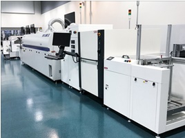
Saki Corp. has partnered with Fuji America to incorporate its 3D automated optical inspection (AOI) and 3D solder paste inspection (SPI) systems into Fuji's Smart Factory SMT line at its Vernon Hills, Illinois facility. Saki's inspection and measurement systems will be used to ensure that the printed circuit boards produced at Fuji adhere to the highest standards of quality and reliability.
"Saki has been on the forefront of innovation for over 20 years, and their inspection systems have played a vital role in the assembly process," said Scott Wischoffer, marketing manager at Fuji America. "As the industry has moved towards the Smart Factory Model and Industry 4.0, our industry partner companies have collaborated to produce an efficient assembly process that will benefit our customers and their customers as well. We are proud to have Saki as part of this Fuji Smart Factory Family."
Saki's BF-3Di AOI system precisely inspects and measures the height of all devices on a printed circuit board and detects defects such as lifted leads, tombstones, reverses, and height variations at high speeds and cycle times. Saki's 3D BF-3Si SPI system is one of the world's fastest 2-projector solder paste inspection systems available. Its Phase Measurement Profilometry with Liquid Crystal on Silicon (LCoS) technology ensures high repeatability of inspection results.
Saki is part of Fuji Machine Manufacturing's Smart Factory with Nexim initiative that standardizes the communication protocol between Saki's SPI and AOI machines and Fuji's component placement machines to create a manufacturing line that extends beyond the boundaries of corporations. This significantly contributes to the production of high quality products and results in a more highly efficient process.
"Saki is pleased to have its AOI and SPI machines installed in the Fuji America Technical Center," said Satoshi Otake, general manager of SAKI America. "It gives us the opportunity to demonstrate the performance and accuracy of our equipment and how it works with Fuji's systems."
About Saki Corp.
Since its inception in 1994, Saki has led the way in the development of automatic recognition through robotic vision technology, applying ground-breaking image processing tools to solve inspection problems associated with printed circuit board assembly. Saki Corporation has headquarters in Tokyo, Japan with offices and sales and support centers around the world. Saki has Quality Management System JIS Q 9001:2008 and ISO 9001:2008 certifications.
Share on:


Testimonial
"In a year when every marketing dollar mattered, I chose to keep I-Connect007 in our 2025 plan. Their commitment to high-quality, insightful content aligns with Koh Young’s values and helps readers navigate a changing industry. "
Brent Fischthal - Koh YoungSuggested Items
AQUANOX A4727 and A4625 Lead KYZEN Offerings at SMTA Oregon Expo and Tech Forum
05/06/2026 | KYZENKYZEN, the global leader in innovative environmentally responsible cleaning chemistries, will exhibit at the SMTA Oregon Expo and Tech Forum scheduled to take place Thursday, May 19 at the Wingspan Event and Conference Center in Hillsboro, Oregon.
Connect the Dots: Designing for the Future of Manufacturing Reality—Surface Finish
05/07/2026 | Matt Stevenson -- Column: Connect the DotsWhen designing the complex boards that many electronic devices require to operate, designers should consider manufacturability at every step. This is my last article focused on designing for the always-evolving manufacturing reality. Choosing the right surface finish has always been important. If you are creating intricate designs with a wide variety of components, like for an ultra-high density interconnect (UHDI) board, surface finish is a critical last step.
Indium to Showcase High-Performance AI Application Solutions at SEMICON SEA 2026
05/01/2026 | Indium CorporationAs a leading provider of advanced materials solutions for today’s demanding AI applications, Indium Corporation® will feature its high-reliability product portfolio at SEMICON SEA 2026, May 5-7, in Kuala Lumpur, Malaysia.
ACCM Unveils Negative and Near-zero CTE Materials for Large-Format AI Chips
04/21/2026 | Advanced Chip and Circuit MaterialsAdvanced Chip and Circuit Materials, Inc. (ACCM) has launched two new materials: Celeritas HM50, with a negative coefficient of thermal expansion (CTE) of -8 ppm/°C to offset the positive CTE and expansion of copper with temperature on circuit boards, and Celeritas HM001, with near-zero CTE and the low-loss performance needed for high-speed signal layers to 224 Gb/s and faster in artificial intelligence (AI) circuits.
SMTA Ultra HDI Symposium, Day 2: Fragile Supply Chains, Fierce Innovation
04/14/2026 | Marcy LaRont, I-Connect007The Arizona weather yielded another beautiful day as we gathered for the second day of SMTA’s annual UHDI symposium. After the first full day discussing the role of AI in business and the how-tos of implementation, Avondale Mayor Mike Pineda kicked off day two, proud to showcase his city and to declare its important place in the continued development of the West Valley, an increasingly important area for tech and manufacturing.