-
- News
- Books
Featured Books
- smt007 Magazine
Latest Issues
Current IssueWhat's Your Sweet Spot?
Are you in a niche that’s growing or shrinking? Is it time to reassess and refocus? We spotlight companies thriving by redefining or reinforcing their niche. What are their insights?
Moving Forward With Confidence
In this issue, we focus on sales and quoting, workforce training, new IPC leadership in the U.S. and Canada, the effects of tariffs, CFX standards, and much more—all designed to provide perspective as you move through the cloud bank of today's shifting economic market.
Intelligent Test and Inspection
Are you ready to explore the cutting-edge advancements shaping the electronics manufacturing industry? The May 2025 issue of SMT007 Magazine is packed with insights, innovations, and expert perspectives that you won’t want to miss.
- Articles
- Columns
- Links
- Media kit
||| MENU - smt007 Magazine
Dr. Mike Bixenman Selected for Best of Conference Award for BTC/QFN Research Presented during SMTAI
January 17, 2017 | KyzenEstimated reading time: 1 minute

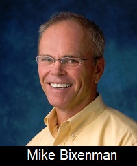
KYZEN is pleased to announce that one of Dr. Mike Bixenman’s papers that was presented during SMTA International 2016 has been selected by the SMTA for a Best Paper Award. Dr. Bixenman won the Rich Freiberger Best of Conference Award for his presentation entitled “BTC/QFN Test Board Design Considerations and Method for Qualifying Soldering Materials and Cleaning Processes.” Bixenman co-authored the paper with Mark McMeen and Jason Tynes from STI Electronics.
The award is based on the conference attendees’ rating of each speaker at the technical session. As a veteran speaker at SMTA International, Dr. Bixenman makes contributions to the industry by sharing his research and findings.
It becomes necessary from time to time to change materials of construction, manufacturing processes, and process conditions. A soldering material or cleaning agent may become unavailable due to environmental regulation, market forces, or reformulation. Certain conditions require some form of verification and validation that the process meets the Original Equipment Manufacturers (OEMs) quality and reliability specifications.
J-STD-001 Requirements for Soldered Electrical and Electronic Assemblies states that validation and verification be confirmed with test vehicles that are representative of the product being produced. Many of the industry standard test vehicles are dated and not representative of current electrical and electronic assemblies.
The purpose of this research is to use a non-standard test board with sensors placed at the bottom termination to study cleanliness and contamination effects under QFN components. The non-standard test board has features to also study thermal paddle design options and to develop a risk profile. This research will report Surface Insulation Resistance effects at the source of the residue.
Dr. Mike Bixenman, CTO of KYZEN, has more than 20 years of experience in the design of electronic assembly cleaning materials and process integration. He was the chair of the 2008 IPC/SMTA Cleaning Symposium and is the current chair of the IPC Cleaning Handbook Task Group. Dr. Bixenman holds four earned degrees including a Doctorate in Business Administration.
The authors will formally be presented their awards at the Opening Ceremony during SMTA International on Sept. 19, 2017 in Rosemont, Illinois. The papers are available in the conference proceedings available in the SMTA Bookstore.
Testimonial
"Our marketing partnership with I-Connect007 is already delivering. Just a day after our press release went live, we received a direct inquiry about our updated products!"
Rachael Temple - AlltematedSuggested Items
Ansys 2025 R2 Enables Next-Level Productivity by Leveraging AI, Smart Automation, and Broader On-Demand Capabilities
07/30/2025 | PRNewswireAnsys, now part of Synopsys, announced 2025 R2, featuring new AI-powered capabilities across the portfolio that accelerate simulation and expand accessibility.
Target Condition: The 5 Ws of PCB Design Constraints
07/29/2025 | Kelly Dack -- Column: Target ConditionHave you ever sat down to define PCB design constraints and found yourself staring at a settings window with more checkboxes than a tax form? You’re not alone. For many designers—especially those newer to the layout world—the task of setting up design constraints can feel like trying to write a novel in a language you just started learning.
Zuken to Showcase Defence & Security-Focused Electronic Systems Design Solutions at DSEI 2025
07/24/2025 | ZukenZuken, a global leader in electronic and electrical design automation, will showcase its latest innovations for defence and security systems at DSEI 2025, taking place at ExCeL London from 9–12 September 2025.
Creating a Design Constraint Strategy
07/24/2025 | I-Connect007 Editorial TeamMost designers learn how to set their design constraints through trial and error. EDA vendors’ guidelines explain how to use their particular tools’ constraints, and IPC standards offer a roadmap, but PCB designers usually develop their own unique styles for setting constraints. Is there a set of best practices for setting constraints? That’s what I asked Global Electronics Association design instructor Kris Moyer, who covers design constraints in his classes.
Elementary Mr. Watson: Closing the Gap Between Design and Manufacturing
07/23/2025 | John Watson -- Column: Elementary, Mr. WatsonModern PCB designers are not merely engineers or technicians. I believe that PCB design, at its core, is an art form, and modern PCB designers should be considered artists. Beyond the technical calculations and engineering rules lies a creative process that involves vision, balance, and a passion for what we do. Like any artist who works with brush and canvas or chisel and stone, a PCB designer shapes invisible pathways that bring ideas to life. Each trace, layer, and component placement reflects thoughtful decisions that blend form, fit, and function.