


 Dan’s Biz Bookshelf: ‘Elevate: Push Beyond Your Limits'
 The Marketing Minute: The First Step to More Sales—Marketing
 It’s Only Common Sense: Customer Service Is Sales in Disguise


Nano Dimension Combines Electronic Components within PCBs as part of the Printing Process
January 30, 2017 | Nano Dimension Ltd.Estimated reading time: 1 minute
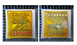
Nano Dimension Ltd., a leader in the field of 3D printed electronics, announced today that its wholly owned subsidiary, Nano Dimension Technologies Ltd., has successfully 3D printed electrical circuits, in which it embedded electrical components, through placement, as an integral part of the printing process. The company's 3D printer - the DragonFly 2020 - enables 3D printing of PCBs with conductive ink and dielectric ink.
Today, the company announced a successful proof of concept of PCBs inkjet printing, in which electrical components were placed during the printing process. The method presents several advantages:
- It improves the PCB reliability by maintaining the electronic components internally and keeping them from being exposed to the external environment, while protecting them from mechanical, temperature, and corrosion damages.
- It makes obsolete the soldering process since the components are embedded within the printed board during printing. The connectivity between components then takes place as part of the 3D printing process without the need for a mediating soldering material.
- The new process enables printing on electronics components without their complete packaging (printing directly on the dye), and consequently supports the creation of thinner, more protected PCBs.
This new and significant capability is expected to become supported in future versions of Nano Dimension's 3D printers.
The company has filed a patent application with the U.S. Patent and Trademark Office for this unique development, which the company believes is significant for a wide range of industry sectors such as defense, space, consumer products, telco, and more.
About Nano Dimension Ltd.
Nano Dimension, founded in 2012, focuses on development of advanced 3D printed electronics systems and advanced additive manufacturing. Nano Dimension's unique products combine three advanced technologies: 3D inkjet, 3D software, and nanomaterials. The company's primary products include the first 3D printer dedicated to printing multi-layer PCBs (printed circuit boards), and advanced nanotechnology-based conductive and dielectric inks.
In addition to the trading of the company's American Depositary Shares on NASDAQ, the company's ordinary shares are also traded on the TASE in Israel. The Bank of New York Mellon serves as the depositary for Nano Dimension.
Share on:


Suggested Items
Silicon Mountain Contract Services Enhances SMT Capabilities with New HELLER Reflow Oven
07/17/2025 | Silicon Mountain Contract ServicesSilicon Mountain Contract Services, a leading provider of custom electronics manufacturing solutions, is proud to announce a significant upgrade to its SMT production capability with the addition of a HELLER 2043 MK5 10‑zone reflow oven to its Nampa facility.
SHENMAO Strengthens Semiconductor Capabilities with Acquisition of PMTC
07/10/2025 | SHENMAOSHENMAO America, Inc. has announced the acquisition of Profound Material Technology Co., Ltd. (PMTC), a premier Taiwan-based manufacturer of high-performance solder balls for semiconductor packaging.
Hands-On Demos Now Available for Apollo Seiko’s EF and AF Selective Soldering Lines
06/30/2025 | Apollo SeikoApollo Seiko, a leading innovator in soldering technology, is excited to spotlight its expanded lineup of EF and AF Series Selective Soldering Systems, now available for live demonstrations in its newly dedicated demo room.
SolderKing’s Successful Approach to Modern Soldering Needs
06/18/2025 | Nolan Johnson, I-Connect007Chris Ward, co-founder of the family-owned SolderKing, discusses his company's rapid growth and recent recognition with the King’s Award for Enterprise. Chris shares how SolderKing has achieved these award-winning levels of service in such a short timeframe. Their secret? Being flexible in a changing market, technical prowess, and strong customer support.
E-tronix Announces Upcoming Webinar with ELMOTEC: Optimizing Soldering Quality and Efficiency with Robotic Automation
05/30/2025 | E-tronixE-tronix, a Stromberg Company, is excited to host an informative webinar presented by Raphael Luchs, CEO of ELMOTEC, titled "Optimize Soldering Quality and Efficiency with Robotic Automation," taking place on Wednesday, June 4, 2025 at 12:00 PM CDT.