-
- News
- Books
Featured Books
- smt007 Magazine
Latest Issues
Current IssueIntelligent Test and Inspection
Are you ready to explore the cutting-edge advancements shaping the electronics manufacturing industry? The May 2025 issue of SMT007 Magazine is packed with insights, innovations, and expert perspectives that you won’t want to miss.
Do You Have X-ray Vision?
Has X-ray’s time finally come in electronics manufacturing? Join us in this issue of SMT007 Magazine, where we answer this question and others to bring more efficiency to your bottom line.
IPC APEX EXPO 2025: A Preview
It’s that time again. If you’re going to Anaheim for IPC APEX EXPO 2025, we’ll see you there. In the meantime, consider this issue of SMT007 Magazine to be your golden ticket to planning the show.
- Articles
- Columns
Search Console
- Links
- Media kit
||| MENU - smt007 Magazine
Saki to Demo Advanced 3D AOI Capabilities at NEPCON China
April 13, 2017 | Saki CorporationEstimated reading time: 1 minute

Saki Corporation will demonstrate the advanced capabilities and new extra component detection (ECD) feature of its BF-3Di 3D automated optical inspection (AOI) systems at NEPCON China on April 25-27, 2017 at the Shanghai World EXPO Exhibition & Convention Center in Shanghai, China, in booth 1J25.
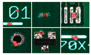
Saki's ECD algorithm inspects for stray components, solder balls, and foreign materials across the entire surface of the circuit board and can detect objects of 200 microns or less, thereby eliminating these defects. ECD, coupled with the benefits of the complete scan of the PCB by Saki's line scan technology, provides further assurance of product quality. Saki's ECD is incorporated into both its 2D and 3D AOI systems.
Saki's systems handle all types of boards, including extra-large (686x870mm) PCBs. The BF-3 Di series uses multi-phase ring lighting and Saki's proprietary coaxial top light illumination to measure the solder height and accurately reconstruct the fillet geometry of the image. With the newly developed 4-way side cameras, it accurately detects J-leads, QFN packages, and connector assemblies via 4-way projection technology. These systems measure heights from 0-20mm with 1µm resolution and achieve full automation with very low false calls and zero escapes. In addition, Saki's BF-3 Di software reduces library creation time by over 50% when compared to conventional AOI machines.
About Saki Corporation
Since its inception in 1994, Saki has led the way in the development of automatic recognition through robotic vision technology, applying ground-breaking image processing tools to solve inspection problems associated with printed circuit board assembly. Saki Corporation has headquarters in Tokyo, Japan with offices and sales and support centers around the world. Saki has Quality Management System JIS Q 9001:2008 and ISO 9001:2008 certifications. For more information click here.
Suggested Items
Indium’s Karthik Vijay to Present on Dual Alloy Solder Paste Systems at SMTA’s Electronics in Harsh Environments Conference
05/06/2025 | Indium CorporationIndium Corporation Technical Manager, Europe, Africa, and the Middle East Karthik Vijay will deliver a technical presentation on dual alloy solder paste systems at SMTA’s Electronics in Harsh Environments Conference, May 20-22 in Amsterdam, Netherlands.
SolderKing Achieves the Prestigious King’s Award for Enterprise in International Trade
05/06/2025 | SolderKingSolderKing Assembly Materials Ltd, a leading British manufacturer of high-performance soldering materials and consumables, has been honoured with a King’s Award for Enterprise, one of the UK’s most respected business honours.
Knocking Down the Bone Pile: Gold Mitigation for Class 2 Electronics
05/07/2025 | Nash Bell -- Column: Knocking Down the Bone PileIn electronic assemblies, the integrity of connections between components is paramount for ensuring reliability and performance. Gold embrittlement and dissolution are two critical phenomena that can compromise this integrity. Gold embrittlement occurs when gold diffuses into solder joints or alloys, resulting in mechanical brittleness and an increased susceptibility to cracking. Conversely, gold dissolution involves the melting away of gold into solder or metal matrices, potentially altering the electrical and mechanical properties of the joint.
'Chill Out' with TopLine’s President Martin Hart to Discuss Cold Electronics at SPWG 2025
05/02/2025 | TopLineBraided Solder Columns can withstand the rigors of deep space cold and cryogenic environments, and represent a robust new solution to challenges facing next generation large packages in electronics assembly.
BEST Inc. Reports Record Demand for EZReball BGA Reballing Process
05/01/2025 | BEST Inc.BEST Inc., a leader in electronic component services, is pleased to announce they are experiencing record demand for their EZReball™ BGA reballing process which greatly simplifies the reballing of ball grid array (BGA) and chip scale package (CSP) devices.