-
- News
- Books
Featured Books
- smt007 Magazine
Latest Issues
Current IssueWhat's Your Sweet Spot?
Are you in a niche that’s growing or shrinking? Is it time to reassess and refocus? We spotlight companies thriving by redefining or reinforcing their niche. What are their insights?
Moving Forward With Confidence
In this issue, we focus on sales and quoting, workforce training, new IPC leadership in the U.S. and Canada, the effects of tariffs, CFX standards, and much more—all designed to provide perspective as you move through the cloud bank of today's shifting economic market.
Intelligent Test and Inspection
Are you ready to explore the cutting-edge advancements shaping the electronics manufacturing industry? The May 2025 issue of SMT007 Magazine is packed with insights, innovations, and expert perspectives that you won’t want to miss.
- Articles
- Columns
- Links
- Media kit
||| MENU - smt007 Magazine
Microtronic to Show Sonix ECHO Scanning Acoustic Microscope at SMT Hybrid Packaging
April 18, 2017 | Microtronic GmbHEstimated reading time: 1 minute

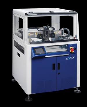
Microtronic GmbH today announced plans to show the Sonix ECHO™ scanning acoustic microscope in Stand 221j in Hall 5 at SMT Hybrid Packaging, scheduled to take place May 16-18, 2017 in Nuremburg, Germany. The ECHO enables package inspection of stacked dies, complex flip chips and more traditional plastic packages.
The ECHO VS adds industry-leading features for the clearest imaging of Cu pillars, molded flip chip (MUF), CSP, MCM, stacked die, hybrids, and other advanced package inspection applications. The ECHO Pro adds fully automated handling for 100 percent package inspection in high-volume production environments.
Ernst J. M. Eggelaar, President of Microtronic commented, “We are excited to present the latest developments and features of the Sonix ECHO to our customers. The system offers many new and cutting-edge features.”
About Microtronic
Microtronic was founded in 1981 and is based near Munich, Germany. With 30 years’ experience, we are the microelectronics leaders in Europe and offer a wide range of products and services to the microelectronics industries. We run regular training courses on various topics through in-house training or can arrange for specific employee training courses on request to suit your needs.
Our customers include companies who require added solderability test, ultrasonic microscopes, circuit board repair systems, welding systems, solders and solder pastes. We offer centralised pricing to our customers with the added benefit of unparalleled delivery times from our centralized European warehouses.
For more information, please click here.
Suggested Items
Driving Innovation: Direct Imaging vs. Conventional Exposure
07/01/2025 | Simon Khesin -- Column: Driving InnovationMy first camera used Kodak film. I even experimented with developing photos in the bathroom, though I usually dropped the film off at a Kodak center and received the prints two weeks later, only to discover that some images were out of focus or poorly framed. Today, every smartphone contains a high-quality camera capable of producing stunning images instantly.
Hands-On Demos Now Available for Apollo Seiko’s EF and AF Selective Soldering Lines
06/30/2025 | Apollo SeikoApollo Seiko, a leading innovator in soldering technology, is excited to spotlight its expanded lineup of EF and AF Series Selective Soldering Systems, now available for live demonstrations in its newly dedicated demo room.
Indium Corporation Expert to Present on Automotive and Industrial Solder Bonding Solutions at Global Electronics Association Workshop
06/26/2025 | IndiumIndium Corporation Principal Engineer, Advanced Materials, Andy Mackie, Ph.D., MSc, will deliver a technical presentation on innovative solder bonding solutions for automotive and industrial applications at the Global Electronics A
Fresh PCB Concepts: Assembly Challenges with Micro Components and Standard Solder Mask Practices
06/26/2025 | Team NCAB -- Column: Fresh PCB ConceptsMicro components have redefined what is possible in PCB design. With package sizes like 01005 and 0201 becoming more common in high-density layouts, designers are now expected to pack more performance into smaller spaces than ever before. While these advancements support miniaturization and functionality, they introduce new assembly challenges, particularly with traditional solder mask and legend application processes.
Knocking Down the Bone Pile: Tin Whisker Mitigation in Aerospace Applications, Part 3
06/25/2025 | Nash Bell -- Column: Knocking Down the Bone PileTin whiskers are slender, hair-like metallic growths that can develop on the surface of tin-plated electronic components. Typically measuring a few micrometers in diameter and growing several millimeters in length, they form through an electrochemical process influenced by environmental factors such as temperature variations, mechanical or compressive stress, and the aging of solder alloys.