


 Global Citizenship: Together for a Perfect PCB Solution
 Smart Automation: Odd-form Assembly—Dedicated Insertion Equipment Matters
 Nolan’s Notes: Everyone Has Their Eye on India


Voiding Control at High-Power Die-Attach Preform Soldering
May 17, 2017 | Dr. Arnab Dasgupta, Elaina Zito, and Dr. Ning-Cheng Lee, Indium CorporationEstimated reading time: 4 minutes
Assembly of components with large pads, such as high-brightness LEDs or high-power dies, often is soldered with preforms. Solder preforms are used to lower voiding and to lower flux fumes that can be generated by solder paste. The use of solder preforms also result in better thermal and electrical conductivity compared to Ag epoxy. This is particularly true when the joints are to be formed within a cavity.
Voiding in the solder joint is a concern for high-reliability and high-performance devices. In this study, voiding behavior of large pad high-power devices was simulated with copper (Cu) coupon to Cu coupon sandwiches. A flux-coated preform was studied in this assembly, with variation in solder alloy type, quantity of solid flux coated on solder preform, Cu coupon pre-oxidation extent, reflow temperature, and pressure exerted onto the sandwich during reflow.
Experiment
1. Solder Alloy Type
Preforms of three solder alloys were tested: 96.5Sn/3Ag/0.5Cu (SAC305), 63Sn/37Pb, and 57Bi/42Sn/1Ag. The preform diameter was 0.906-inch, and 0.006-inch thick.
2. Flux Coating
The preform was pre-coated with a solid flux film using liquid flux at 0.5, 1.0, and 2% flux concentrations in isopropyl alcohol upon application.
3. Cu Coupon Oxidation Pre-treatment
The copper coupon (0.906-inch diameter, 0.020-inch thick) was used to simulate both die and substrate. It was pre-cleaned by soaking in a diluted HBF4 aqueous solution, followed by deionized water rinsing, and air drying. These cleaned Cu coupons were then oxidized by placing them on a 230°C hot plate for 0, 30, and 60 seconds, and five minutes prior to the soldering process.
4. Die-Attach Sandwich Setup
The high-power die-attach setup was simulated with the use of two Cu coupons, which were to be joined with a flux-coated solder preform. A 3-inch x 3-inch ceramic plate was used as a carrier. The simulated die-attach sandwich (Cu coupon on a solder preform, then placed on another Cu coupon) was placed on the carrier. At die-attach with solder preforms, many manufacturing processes use fixtures with some weight on the die to secure the sandwich. In this study, metal weight varying from 0 to 100 grams was placed on the top of the sandwich to simulate the fixture weight. Paper cardboard was placed on top of the die for heat insulation, if a weight was used.
5. Reflow Peak Temperature
The sandwich on the carrier was placed on a 5-zone, in-line contact reflow oven, and then sent through the reflow oven with various peak temperatures as follows:
- SAC305: 240°C, 250°C, and 260°C
- 63Sn/37Pb: 205°C, 215°C, and 225°C
- 57Bi/42Sn/1Ag: 160°C, 170°C, and 180°C
6. Reflow Under Various Pressures
For SAC305, various weights were placed on top of the sandwiches at reflow: 0, 10, 30, and 100 grams. For this set of assembly, freshly cleaned Cu coupons, 0.5% flux concentration, and a peak temperature of 240°C were used. Ten sandwiches were reflowed for each condition. For 63Sn/37Pb and 57Bi/42Sn/1Ag, 0, 10, 20, and 30 grams of weight were used for the pressure study.
7. Assessment
After reflow, the sandwiches were examined under X-ray to determine the voiding area percentage. For SAC305, three sandwiches for each weight condition were cross-sectioned to determine the bondline thickness under various weights
Results
Effect of Weight on SAC305 System Using X-ray Images
Figure 1 shows the X-ray images of SAC305 sandwiches under various weights. Here, the flux concentration was 0.5%, the peak temperature was 240°C, and the coupons were etch-cleaned prior to use. Although 10 samples were prepared for each combination of conditions, three sandwiches were removed due to large opens in the solder joints because the image analysis software was unable to determine the voiding percentage properly. Most of the samples showed full wetting to the perimeter of coupons, and only a few showed a small fraction of non-wetting near the edge of the joints.
Figure 1: X-ray images for SAC305 soldered sandwiches processed with various weights on top of samples.
Most of the voids showed plain vacancy, except for a few samples where some spotty light-colored solder were seen within the voids, such as in the third image of the 10-gram series and the first image of the 30-gram series. The spotty solder islands were attributed to the once-formed liquid joints, but were wiped out partially by expanding voids.
In most images, concentric ring textures can be seen clearly, indicating the Cu coupons may be warped. Also, the joint appeared to be thicker toward the center, and the solidification may have been developed stepwise from the edge toward the center.
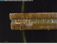
1. Bondline Thickness (BLT): The 100-gram weight samples showed a much lighter shade of color than the other three weight samples, suggesting much thinner solder BLT data for SAC305 joints under various weights. The sandwich samples were cross-sectioned, as exemplified in Figure 2, with the BLT measured at both the edges and the center. The average value was calculated to represent the BLT of a given weight condition.
Page 1 of 3
Share on:


Testimonial
"The I-Connect007 team is outstanding—kind, responsive, and a true marketing partner. Their design team created fresh, eye-catching ads, and their editorial support polished our content to let our brand shine. Thank you all! "
Sweeney Ng - CEE PCBSuggested Items
Koh Young, Fuji, and Kurtz ERSA Drive Smart Manufacturing Solutions for EV and Automotive Electronics at Kunshan, China Technical Seminar
09/11/2025 | Koh YoungKoh Young Technology, the global leader in True 3D measurement-based inspection solutions, partnered with Fuji Corporation and Kurtz ERSA to host an exclusive technical seminar for leading automotive manufacturers in East China. Held on September 4 at Fuji’s factory in Kunshan, the event gathered participants representing over 35 companies.
MacDermid Alpha Presents at SMTA New Delhi, Bangalore Chapter, on Flux–OSP Interaction
09/09/2025 | MacDermid Alpha Electronics SolutionsMacDermid Alpha contributes technical insights on OSP solderability at the Bangalore Chapter, SMTA reinforcing commitment to knowledge-sharing and industry collaboration.
Electra’s ElectraJet EMJ110 Inkjet Soldermask Now in Black & Blue at Sunrise Electronics
09/08/2025 | Electra Polymers LtdFollowing the successful deployment of Electra’s Green EMJ110 Inkjet Soldermask on KLA’s Orbotech Neos™ platform at Sunrise Electronics in Elk Grove Village, Illinois, production has now moved beyond green.
Absolute EMS: The Science of the Perfect Solder Joint
09/05/2025 | Absolute EMS, Inc.Absolute EMS, Inc., a six-time award-winning provider of fast turnaround, turnkey contract electronic manufacturing services (EMS), is drawing attention to the critical role of 3D Solder Paste Inspection (SPI) in ensuring the reliability of both FLEX and rigid printed circuit board assemblies (PCBAs).
Indium Corporation to Highlight High-Reliability Solder Solutions at SMTA Guadalajara Expo
09/04/2025 | Indium CorporationIndium Corporation, a leading materials refiner, smelter, manufacturer, and supplier to the global electronics, semiconductor, thin-film, and thermal management markets, will feature a range of innovative, high-reliability solder products for printed circuit board assembly (PCBA) at the SMTA Guadalajara Expo and Tech Forum, to be held September 17-18 in Guadalajara, Mexico.