


 Target Condition: Distribution of Power—Denounce the Ounce
 Fresh PCB Concepts: Resilience and Renewal in Domestic PCB Manufacturing
 Designers Notebook: Power and Ground Distribution Basics


Seeking out New Functions for Superconducting Nanoelectronics
June 16, 2017 | University of TokyoEstimated reading time: 2 minutes
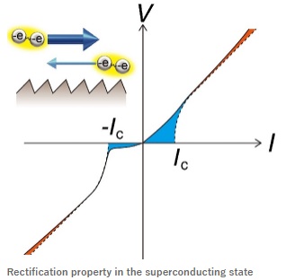
A team of researchers at the University of Tokyo and their collaborators discovered that a two-dimensional semiconductor with a broken inversion symmetry demonstrates rectification, or the property of a diode, under a magnetic field applied in a certain direction. This finding provides important insights essential for developing the next generation of superconducting nanoelectronic materials.
In general, a magnetic field applied in a specific direction in a system in which the spatial inversion symmetry is broken generates rectifying characteristics, but the rectification property is larger in the superconducting state, compared to the normal conducting state. 2017 Ryohei Wakatsuki, Yu Saito.
Superconductivity is a property in which electrical resistance disappears; it has been the focus of much basic and applied research around the world as a next-generation technology that could enhance energy conservation. The integration of superconductors is expected to play an important role in next-generation computing systems, such as in the area of superconducting quantum bits; thus, there is much demand for the development of new functions of superconducting nanoelectronics for these purposes—especially superconductors with a rectifying property, i.e., superconducting diodes. Although recent research has revealed rectification in a normal conductor crystal with a broken inversion symmetry, not much research has been conducted on the rectification property of a superconductor lacking inversion symmetry.
The research group led by graduate students Ryohei Wakatsuki and Yu Saito, Professor Yoshihiro Iwasa, and Professor Naoto Nagaosa at the Graduate School of Engineering, the University of Tokyo, and their collaborators fabricated an electric double-layer transistor (EDLT) structure, a kind of field effect transistor, using a high-quality single crystal of molybdenum disulfide (MoS2), a layered material that is a type of atomic film material. The capacity of electrons induced by the strong electric field to accumulate on the surface of a single crystal of MoS2 in this structure makes it possible to realize synthetically the extremely thin, one-atomic-layer-thick ultimate two-dimensional superconductivity. In the current study, the researchers measured the electric conduction characteristics of a MoS2-EDLT device with a magnetic field applied perpendicular to the surface. They observed extremely large rectifying characteristics in the superconducting state by measuring the second harmonic component of electric resistance to examine rectification.
Moreover, the scientists applied theoretical calculations for superconducting fluctuation currents to explain the mechanism of the enhanced rectification property, and showed that the phenomenon could occur in any superconductor with a broken inversion symmetry.
"The nonlinear response of rectifying characteristics and electric current discovered in this research is considered to be a universal phenomenon in superconductors in which the spatial inversion symmetry has been broken," says Professor Nagaosa. He continues, "The present result will pave the way for the development of functions of superconducting nanoelectronics, as well as become the cornerstone of a new academic field created to study two-dimensional superconductivity with broken spatial inversion symmetry."
Share on:


Testimonial
"In a year when every marketing dollar mattered, I chose to keep I-Connect007 in our 2025 plan. Their commitment to high-quality, insightful content aligns with Koh Young’s values and helps readers navigate a changing industry. "
Brent Fischthal - Koh YoungSuggested Items
Argonne Expands Nation’s AI Infrastructure With Powerful New Supercomputers and Public-Private Partnerships
10/29/2025 | BUSINESS WIREThe U.S. Department of Energy (DOE), Argonne National Laboratory, NVIDIA and Oracle announced a landmark public-private partnership to deliver the DOE’s largest AI supercomputer and accelerate scientific discovery.
HPE Now Powers New AI-Ready Supercomputer Set to Transform Environmental Forecasting in New Zealand
09/22/2025 | BUSINESS WIREHPE announced that Earth Sciences New Zealand (formally NIWA) of Aotearoa (New Zealand) selected HPE Cray XD2000, purpose-built for AI and simulation workloads, to accelerate the organization’s environmental science and precision of meteorological forecasting.
PC Graphics Add-in Board Shipments Up 27% QoQ in 2Q25
09/03/2025 | Jon Peddie ResearchAccording to a new research report from the analyst firm Jon Peddie Research, the growth of the global PC-based graphics add-in board market reached 11.6 million units in Q2'25 and desktop PC CPUs shipments increased to 21.7 million units.
PC GPU Shipments Up 8.4% in 2Q25 on Pre-Tariff Demand
09/02/2025 | Jon Peddie ResearchJon Peddie Research reports the growth of the global PC-based graphics processor unit (GPU) market reached 74.7 million units in Q2'25, and PC CPU shipments increased to 66.9 million units.
20 Years of Center Nanoelectronic Technologies (CNT) – Backbone of German Semiconductor Research Celebrates Anniversary
08/14/2025 | Fraunhofer IPMSThe Center Nanoelectronic Technologies (CNT) of the Fraunhofer Institute for Photonic Microsystems (IPMS) is celebrating its 20th anniversary this year. Since its founding in 2005, it has developed into a pillar of applied semiconductor research in Germany and Europe. With its unique research cleanroom and equipment adhering to the 300-mm wafer industry standard, CNT is unparalleled in Germany and serves as a central innovation driver for the microelectronics industry.