-

- News
- Books
Featured Books
- smt007 Magazine
Latest Issues
Current Issue
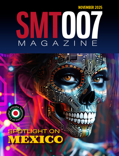
Spotlight on Mexico
Mexico isn’t just part of the electronics manufacturing conversation—it’s leading it. From growing investments to cross-border collaborations, Mexico is fast becoming the center of electronics in North America. This issue includes bilingual content, with all feature articles available in both English and Spanish.

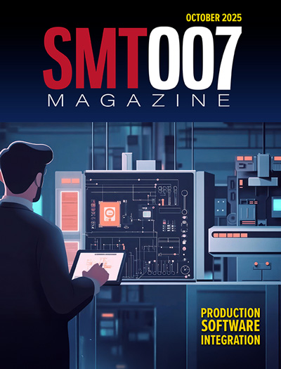
Production Software Integration
EMS companies need advanced software systems to thrive and compete. But these systems require significant effort to integrate and deploy. What is the reality, and how can we make it easier for everyone?

Spotlight on India
We invite you on a virtual tour of India’s thriving ecosystem, guided by the Global Electronics Association’s India office staff, who share their insights into the region’s growth and opportunities.
- Articles
Article Highlights
- Columns
- Links
- Media kit
||| MENU - smt007 Magazine
Summit Interconnect's Gerry Partida to Present at SMTA Capital Expo and Tech Forum
August 7, 2017 | SMTAEstimated reading time: 1 minute
Gerry Partida of Summit Interconnect will present "Density, Advanced Materials and Cost Drivers Associated with Advanced Circuit Design, Fabrication and Assembly" at the upcoming SMTA Capital Expo and Tech Forum, to be held on August 24 at Johns Hopkins University/Applied Physics Lab, Kossiakoff Center.
PCBs are the platform for all surface mount technology processes and electronics manufacturing. There have been tremendous advancements in high speed and microwave materials, via structures and processing techniques. The material constructions and attributes provide unique opportunities for designers and unique challenges for bare printed circuit board fabricators. Partida will explore the various material options and their trade-offs, provide insight into the manufacture of multiple lamination cycle requirements, review stack-up and routing considerations, managing registration requirements, micro drilling and copper wrap plating processes. This will be an invaluable session to understand materials considerations, cost trade-offs and leading-edge processing technologies for the design, manufacture and assembly of high-technology printed circuit boards.
The SMTA Capital Expo and Tech Forum will be held at Johns Hopkins University/Applied Physics Lab, Kossiakoff Center, 11100 Johns Hopkins Road, Laurel, Maryland. Registration opens at 8:00 am and includes a complimentary lunch on the show floor. Exhibits are open from 9:00 am until 3:00 pm and the first technical presentation will start at 9:30 am.
To register for this free event, click here.
About Surface Mount Technology Association (SMTA)
The SMTA membership is an international network of professionals who build skills, share practical experience and develop solutions in electronic assembly technologies, including microsystems, emerging technologies, and related business operations. For more information or to join, please visit www.smta.org.
Testimonial
"Your magazines are a great platform for people to exchange knowledge. Thank you for the work that you do."
Simon Khesin - Schmoll MaschinenSuggested Items
Trouble in Your Tank: Understanding Interconnect Defects, Part 1
11/04/2025 | Michael Carano -- Column: Trouble in Your TankThis month, I’ll address interconnect defects (ICDs). While this defect continues to rear its ugly head, don’t despair. There are solutions, most of which center on process control and understanding the relationship of the chemistry, materials, and equipment. First, though, let’s discuss ICDs.
Target Condition: Distribution of Power—Denounce the Ounce
11/05/2025 | Kelly Dack -- Column: Target ConditionHave you ever wondered why the PCB design segment uses ounces to describe copper thickness? There’s a story behind all of this—a story that’s old, dusty, and more than a little absurd. (Note that I didn’t add “Like many of us.”) Legend has it that back in the days of copper tinkers and roofing tradesmen, the standard was set when a craftsman hammered out a sheet of copper until it weighed one ounce, when its area conveniently matched the square of the king’s foot.
WestDev Announces Advanced Thermal Analysis Integration for Pulsonix PCB Design Suite
10/29/2025 | WestDev Ltd.Pulsonix, the industry-leading PCB design software from WestDev Ltd., announced a major enhancement to its design ecosystem: a direct interface between Pulsonix and ADAM Research's TRM (Thermal Risk Management) analysis software.
Designers Notebook: Power and Ground Distribution Basics
10/29/2025 | Vern Solberg -- Column: Designer's NotebookThe principal objectives to be established during the planning stage are to define the interrelationship between all component elements and confirm that there is sufficient surface area for placement, the space needed to ensure efficient circuit interconnect, and to accommodate adequate power and ground distribution.
Episode 6 of Ultra HDI Podcast Series Explores Copper-filled Microvias in Advanced PCB Design and Fabrication
10/15/2025 | I-Connect007I-Connect007 has released Episode 6 of its acclaimed On the Line with... American Standard Circuits: Ultra High Density Interconnect (UHDI) podcast series. In this episode, “Copper Filling of Vias,” host Nolan Johnson once again welcomes John Johnson, Director of Quality and Advanced Technology at American Standard Circuits, for a deep dive into the pros and cons of copper plating microvias—from both the fabricator’s and designer’s perspectives.


