


 The Government Circuit: New Council Now Helps Shape Policy Decisions in the Electronics Supply Chain
 Learning With Leo: Soldering—The Interpretation Problem
 Nolan’s Notes: The ROI of Setup Optimization


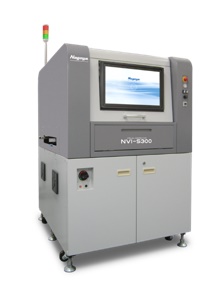
Mek (Marantz Electronics) has launched its latest automated solder paste inspection (SPI) system—the Model S2—which features patented third generation sensor technology that enables unique, simultaneous 2D and 3D inspection. It will be on display for the first time at Productronica in Munich, Hall A2 Booth 402.
The new ISO-Spector S2 utilizes the latest in 12 Mega Pixel camera technology. A fibre optic link allows for a 32 gigabit image data transfer speed.
The S2 delivers the highest quality 2D colour imaging using Episcopic and low angle diffuse RGB lighting systems that remove all specular reflections from solder fluxes and solder mask. Shadow free violet/blue dual lasers provide precise and repeatable 3D images. Available with standard resolution of 18/9µm lens resolution for inspection down to 01005 pad geometries or optionally with 12/6µm for pad geometries down to 008004. On the fly resolution switching allows the efficient inspection of mixed technology PCB’s.
Synthetic color imaging allows the simplification of color extraction of solder mask, silk screen and solder and isolates the solder to be measured, even below zero reference.
The S2 moves SPI forwards from a means of process control to one of production control. Using the Mek S2 and the real-time feedback provided by the SPC-One SPC package the user can narrow tolerances in the print process by adopting automatically to the actual process capability, bringing the real world of printing into its tolerances. Tighter tolerances over the whole PCB, enable the user to monitor process drift which was previously difficult or impossible to capture. This process is especially useful for users of jet style paste printers. The S2 can quickly adjust to changes made in the jetting program without completely reprogramming the inspection parameters. Variations in the jet printing process are immediately visible and fed back.
SPI equipment is essential to monitor and control the most critical, error prone process step in manufacturing defect-free electronic assemblies; solder paste printing. The interception of print defects reduces rework costs, delivers instant yield improvement and accelerates ROI.
About Mek (Marantz Electronics Ltd)
A former division of Marantz well known for its high quality Audio/Video products, Mek Japan (Marantz Electronics Kabushiki Kaisha), developed its first AOI system in 1994. Developed to inspect PCB assemblies for correct component placement and soldering, the company’s original AOI system was designed for use in Marantz factories. Proving to be a highly successful, cost-effective alternative to traditional human inspection, Mek developed its first generation commercial system in 1996. With a steadily growing installed base, MEK Japan and its European/American headquarters, Mek, have sold over 6000 units worldwide to date. Now well established as a leading force in AOI technologies, the company also manufactures a 5D post-print SPI system which combines 3D and 2D image processing methodologies to deliver unprecedented defect detection. At the beginning of March 2014 the company opened US offices in Las Vegas.


