


 Powering the Future: Why True Ceramic Circuits Are Not Just ‘Better PCBs’
 Global Sourcing Spotlight: The Global Quality Gap—Why Consistency Wins the Contract
 Knocking Down the Bone Pile: Precision Milling of Underfilled SMT Components


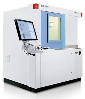
X-ray analysis of circuit boards has now become one of the most important methods in the manufacturing process for quality assurance of soldering, to visually check for pores and voids. The next step is analysis using 3D methods such as laminography and computer tomography. Customers are now able to closely examine their boards in the Technology Center at Rehm Thermal Systems by using the new Y. Cheetah μHD CT X-ray inspection system from YXLON.
Voids have a huge effect on the quality of the solder joint, therefore automotive manufacturers are increasingly setting acceptance limits on components. Not everyone is fortunate enough to have the necessary technical equipment. That is why Rehm Technology Center offers customers the opportunity to thoroughly inspect boards and jointly perfect their processes. A wide range of SMD and inspection equipment can be used under professional supervision for fault management. Solder joints can be examined in detail using the new YXLON Cheetah μHD X-ray inspection system, which enables high-resolution, non-destructive, real-time microfocus X-ray inspection of components and sub-assemblies, circuit boards, electronic and mechanical modules, sensors, MEMS and MOEMS as well as electromechanical components and connectors. It combines several innovative developments, such as fine-focus tube technology, a high-power target, a latest generation long-life finely calibrated flat detector and a manipulator with vibration damping, as well as eHDR inspection, micro CT and micro-laminography.
"Among other things, the radiographs help to evaluate the soldering quality and the void rates. Afterwards, we can make a decision with the customer as to whether any further vacuum processes are necessary and make fine adjustments to these processes. The system also performs the entire spectrum of state-of-the-art X-ray inspections, including laminography and computer tomography. This offers a wide range of manual and automatic inspection opportunities, such as distance measurements, layer assembly, BGA solder joint analysis as well as close inspections of the solder that don’t interfere with structures of components, conductor tracks, substrates and much more. The results obtained form the basis for successfully improving the processes. We particularly value the simplicity, flexibility and above all the accuracy of the system," emphasizes Helmut Öttl, Head of Process Development/Application at Rehm.
Using laminography, it is possible to generate precise layer images of larger or double-sided printed circuit boards as well as of multilayer semiconductor components. In particular, however, industrial computer tomography offers three-dimensional insights into test parts and thus facilitates the analysis of internal structures, dimensional measurements or set-point comparisons to CAD data. In addition to this, computer tomography also provides valuable information for the production process and enables detailed insights into the finest structures and smallest components.
"The YXLON Cheetah microfocus X-ray inspection system offers exactly what customers require: precision, flexibility, ease of use and speed. This is the only way today's modern manufacturing companies can satisfy the growing complexity of electrical and electronic test parts," says Thorsten Rother, YXLON's Market Manager.
The successful cooperation between Rehm and YXLON is the ideal basis for further joint projects with regard to vacuum technology, fault analysis and test methods.
Image: (from left) Helmut Öttl, Head of Process Development/Application (Rehm) and Thorsten Rother, Market Manager (YXLON) in front of the Y. Cheetah μHD X-ray inspection system (picture: Rehm Thermal Systems).
About YXLON International
YXLON International develops and manufactures X-ray and CT inspection systems for a wide range of applications and industries. Whether in the aerospace, automotive or electronics industries, some of the largest manufacturers are YXLON customers who rely on the quality of YXLON worldwide. CT systems have also been part of the product portfolio since 2003. YXLON is right there for their customers worldwide with headquarters in Hamburg and sales and service locations in Tokyo, Hudson (Ohio), San Jose (California), Beijing, Shanghai, Hattingen and Heilbronn as well as a representative network in more than 50 countries. Since 2007, YXLON International has been part of the COMET Group.
About Rehm Thermal System
As a specialist in the field of thermal system solutions for the electronics and photovoltaics industries, Rehm is a technology and innovation leader in the modern and economical production of electronic modules. As a globally operating manufacturer of reflow soldering systems with convection, condensation or vacuum, drying and coating systems, functional test systems, equipment for the metallization of solar cells as well as numerous customer-specific special systems, we are represented in all relevant growth markets and, as a partner with more than 25 years of industry experience, we implement innovative manufacturing solutions that set standards.


