


 It’s Only Common Sense: Customer Service Is Sales in Disguise
 Dan’s Biz Bookshelf: ‘Dream First, Details Later
 Happy’s Tech Talk #40: Factors in PTH Reliability—Hole Voids


Low-Cost Wearables Manufactured by Hybrid 3D Printing
September 8, 2017 | Harvard School of Engineering and Applied SciencesEstimated reading time: 5 minutes
New method combines precision printing of stretchable conductive inks with pick-and-place of electronic components to make flexible, wearable sensors.
A new hybrid 3D printing technique developed at the Wyss Institute at Harvard University, Harvard’s John A. Paulson School of Engineering and Applied Sciences, and the Air Force Research Laboratory combines stretchable conductive inks and electronic components into flexible, durable wearable devices that move with the body and offer increased programmability.
Human skin must flex and stretch to accommodate the body’s every move. Anything worn tight on the body must also be able to flex around muscles and joints, which helps explain why synthetic fabrics like spandex are popular in active wear. Wearable electronic devices that aim to track and measure the body’s movements must possess similar properties, yet integrating rigid electrical components on or within skin-mimicking matrix materials has proven to be challenging. Such components cannot stretch and dissipate forces like soft materials can, and this mismatch in flexibility concentrates stress at the junction between the hard and soft elements, frequently causing wearable devices to fail.
Now, a collaboration between the lab of Jennifer Lewis, Sc.D. at the Harvard John A. Paulson School of Engineering and Applied Sciences (SEAS) and the Wyss Institute for Biologically Inspired Engineering at Harvard University and J. Daniel Berrigan, Ph.D. and Michael Durstock, Ph.D. at the US Air Force Research Laboratory has created a new additive manufacturing technique for soft electronics, called hybrid 3D printing, that integrates soft, electrically conductive inks and matrix materials with rigid electronic components into a single, stretchable device.
“With this technique, we can print the electronic sensor directly onto the material, digitally pick-and-place electronic components, and print the conductive interconnects that complete the electronic circuitry required to ‘read’ the sensor’s data signal in one fell swoop,” says first author Alex Valentine, who was a Staff Engineer at the Wyss Institute when the study was completed and is currently a medical student at the Boston University School of Medicine.
The stretchable conductive ink is made of thermoplastic polyurethane (TPU), a flexible plastic that is mixed with silver flakes. Both pure TPU and silver-TPU inks are printed to create the devices’ underlying soft substrate and conductive electrodes, respectively.
“Because both the substrate and the electrodes contain TPU, when they are co-printed layer-by-layer they strongly adhere to one another prior to drying,” explains Valentine. “After the solvent evaporates, both of the inks solidify, forming an integrated system that is both flexible and stretchable.”
Because the ink and substrate are 3D-printed, we have complete control over where the conductive features are patterned, and can design circuits to create soft electronic devices of nearly every size and shape.
The printing process causes the silver flakes in the conductive ink to align themselves along the printing direction so their flat, plate-like sides layer on top of one another, like overlapping leaves on a forest floor. This structural alignment improves their ability to conduct electricity along the printed electrodes.
“Because the ink and substrate are 3D-printed, we have complete control over where the conductive features are patterned, and can design circuits to create soft electronic devices of nearly every size and shape,” says Will Boley, Ph.D., a postdoctoral researcher in the Lewis lab at SEAS and co-author of the paper.
Soft sensors composed of conductive materials that exhibit changes in their electrical conductivity when stretched (which is how they detect movement) are coupled with a programmable microcontroller chip to process those data, as well as a readout device that communicates the data in a form humans can understand. To achieve this, the researchers combined the printed soft sensors with a digital “pick-and-place process” that applies a modest vacuum through an empty printing nozzle (through which ink is normally dispensed) to pick up electronic components and place them onto the substrate surface in a specific, programmable manner.
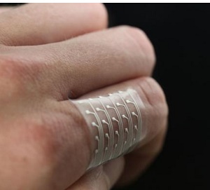
Because these surface-mounted electrical components (e.g., LEDs, resistors, micro-chips) are by nature hard and rigid, the team took advantage of TPU’s adhesive properties by applying a dot of TPU ink beneath each component prior to attaching it to the underlying soft TPU substrate. Once dried, the TPU dots serve to anchor these rigid components and distribute stress throughout the entire matrix, allowing the fully assembled devices to be stretched up to 30 percent while still maintaining function. A device composed of 12 LEDs attached to a flat TPU sheet created using this method was able to be repeatedly bent into a cylindrical shape without reduction in the intensity of the LEDs’ light or mechanical failure of the device.
As a simple proof-of-concept, their team created two soft electronic devices to demonstrate the full capabilities of this additive manufacturing technique. A strain sensor was fabricated by printing TPU and silver-TPU-ink electrodes onto a textile base and applying a microcontroller chip and readout LEDs via the pick-and-place method, resulting in a wearable sleeve-like device that indicates how much the wearer’s arm is bending through successive lighting-up of the LEDs. The second device, a pressure sensor in the shape of a person’s left foot, was created by printing alternating layers of conductive silver-TPU electrodes and insulating TPU to form electrical capacitors on a soft TPU substrate, whose deformation patterns are processed by a manual electrical readout system to make a visual “heat map” image of the foot when a person steps on the sensor.
While the team is continuing to optimize both their materials and their methods, hybrid 3D printing is broadly applicable to manufacturing myriad electronic devices.
“We have both broadened the palette of printable electronic materials and expanded our programmable, multi-material printing platform to enable digital ‘pick-and-place’ of electronic components. We believe that this is an important first step toward making customizable, wearable electronics that are lower-cost and mechanically robust,” says Lewis, who is the corresponding author of the paper, a Core Faculty member at the Wyss Institute, and the Hansjörg Wyss Professor of Biologically Inspired Engineering at SEAS.
Additional authors of the study include Travis Busbee, a graduate student in the Lewis lab and co-founder of Voxel8; Jordan Raney, Ph.D., former postdoc in the Lewis lab and current Assistant Professor in the School of Engineering and Applied Sciences at the University of Pennsylvania; Alex Chortos, Ph.D., and a postdoc in the Lewis lab; Arda Kotikian, a Graduate Research Fellow in the Lewis lab.
This research was supported by the Air Force Research Laboratory Materials and Manufacturing Directorate and UES, the Vannevar Bush Faculty Fellowship Program under the Office of Naval Research, a generous donation from the GETTYLAB, and the Wyss Institute at Harvard University.
Share on:


Suggested Items
Copper Price Surge Raises Alarms for Electronics
07/15/2025 | Global Electronics Association Advocacy and Government Relations TeamThe copper market is experiencing major turbulence in the wake of U.S. President Donald Trump’s announcement of a 50% tariff on imported copper effective Aug. 1. Recent news reports, including from the New York Times, sent U.S. copper futures soaring to record highs, climbing nearly 13% in a single day as manufacturers braced for supply shocks and surging costs.
Symposium Review: Qnity, DuPont, and Insulectro Forge Ahead with Advanced Materials
07/02/2025 | Barb Hockaday, I-Connect007In a dynamic and informative Innovation Symposium hosted live and on Zoom on June 25, 2025, representatives from Qnity (formerly DuPont Electronics), DuPont, and Insulectro discussed the evolving landscape of flexible circuit materials. From strategic corporate changes to cutting-edge polymer films, the session offered deep insight into design challenges, reliability, and next-gen solutions shaping the electronics industry.
Indium Corporation Expert to Present on Automotive and Industrial Solder Bonding Solutions at Global Electronics Association Workshop
06/26/2025 | IndiumIndium Corporation Principal Engineer, Advanced Materials, Andy Mackie, Ph.D., MSc, will deliver a technical presentation on innovative solder bonding solutions for automotive and industrial applications at the Global Electronics A
Gorilla Circuits Elevates PCB Precision with Schmoll’s Optiflex II Alignment System
06/23/2025 | Schmoll MaschinenGorilla Circuits, a leading PCB manufacturer based in Silicon Valley, has enhanced its production capabilities with the addition of Schmoll Maschinen’s Optiflex II Post-Etch Punch system—bringing a new level of precision to multilayer board fabrication.
Day 1: Cutting Edge Insights at the EIPC Summer Conference
06/17/2025 | Pete Starkey, I-Connect007The European Institute for the PCB Community (EIPC) Summer Conference took place this year in Edinburgh, Scotland, June 3-4. This is the second of three articles on the conference. The other two cover the keynote speeches and Day 2 of the technical conference. Below is a recap of the first day’s sessions.