


 Standard of Excellence: The Future of Fabrication—From Art to Automation
 Knocking Down the Bone Pile: The Business Case for Component Reclamation
 Global Sourcing Spotlight: The Hidden Power of the Rep Network


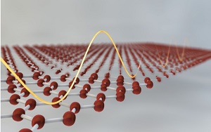
Graphene Flagship researches from CNR-Istituto Nanoscienze, Italy and the University of Cambridge, UK have shown that it is possible to create a terahertz saturable absorber using graphene produced by liquid phase exfoliation and deposited by transfer coating and ink jet printing.
A terahertz saturable absorber decreases its absorption of light in the terahertz range (far infrared) with increasing light intensity and has great potential for the development of terahertz lasers, with applications in spectroscopy and imaging. These high-modulation, mode-locked lasers open up many prospects in applications where short time scale excitation of specific transitions are important, such as time-resolved spectroscopy of gasses and molecules, quantum information or ultra-high speed communication.
“We started working on saturable terahertz absorbers to solve the problem of producing a miniaturized mode-locked terahertz laser with thin and flexible integrated components that also had good modulation” said Graphene Flagship researcher Miriam Vitiello from CNR-Istituto Nanoscienze in Italy.
Graphene is a promising saturable absorber as it has intrinsic broadband operations and ultrafast recovery time along with an ease of fabrication and integration, as first demonstrated in ultra-fast infra-red lasers by Flagship partner University of Cambridge. In the terahertz range, the present paper exploits graphene produced by liquid phase exfoliation, a method ideally suited to mass production, to prepare inks, easily deposited by transfer coating or ink jet printing.
“It was important to us to use a type of graphene that could be integrated into the laser system with flexibility and control” said Vitiello “Ink jet printing along with transfer coating achieved that.”
Using mode-locked lasers to produce ultra fast pulses in the terahertz range can have interesting and exciting uses. “These devices could have applications in medical diagnostics when time of flight topography is of importance – you could see a tumour inside a tissue” said Vitiello.
Frank Koppens, of the Institute of Photonic Sciences in Spain, is the leader of the Graphene Flagship’s Photonics and Optoelectronics Work Package, which focuses on developing graphene-based technologies for imaging and sensing, data transfer and other photonics applications. “This is a new discovery with immediate impact on applications. Clearly, this is a case where graphene beats existing materials in terms of efficiency, scalability, compactness and speed” he said.
Andrea C. Ferrari, Science and Technology Officer of the Graphene Flagship, and Chair of its Management Panel added "It is an important milestone to have demonstrated that easily produced and printable graphene inks can also serve to enable ultrafast lasers in the terahertz range. Since the Flagship’s inception, a variety of lasers have been made covering the visible to IR spectral range, but now the important THz range, with applications in security and medical diagnostic, is finally made accessible by graphene, starting yet another possible application field."
Original by: Sian Fogden


