-
- News
- Books
Featured Books
- pcb007 Magazine
Latest Issues
Current IssueThe Hole Truth: Via Integrity in an HDI World
From the drilled hole to registration across multiple sequential lamination cycles, to the quality of your copper plating, via reliability in an HDI world is becoming an ever-greater challenge. This month we look at “The Hole Truth,” from creating the “perfect” via to how you can assure via quality and reliability, the first time, every time.
In Pursuit of Perfection: Defect Reduction
For bare PCB board fabrication, defect reduction is a critical aspect of a company's bottom line profitability. In this issue, we examine how imaging, etching, and plating processes can provide information and insight into reducing defects and increasing yields.
Voices of the Industry
We take the pulse of the PCB industry by sharing insights from leading fabricators and suppliers in this month's issue. We've gathered their thoughts on the new U.S. administration, spending, the war in Ukraine, and their most pressing needs. It’s an eye-opening and enlightening look behind the curtain.
- Articles
- Columns
- Links
- Media kit
||| MENU - pcb007 Magazine
SnapEDA Launches Instabuild, a Free Computer Vision-Based Part Builder
October 4, 2017 | SnapEDAEstimated reading time: 1 minute

SnapEDA, the Internet’s first parts library for circuit board design, is launching InstaBuild, the first free automated part builder. InstaBuild uses powerful computer vision technology to enable PCB designers to make schematic symbols in mere minutes.
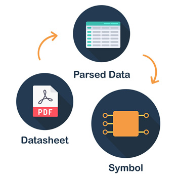
Using a datasheet as the input, it automatically extracts symbol pinouts, understands whether a pin is an input, output or power pin, and auto-arranges the symbols based on SnapEDA’s published symbol standards.
“InstaBuild is based on the underlying technology we use internally at SnapEDA to create parts quickly,” said Natasha Baker, CEO and founder of SnapEDA. “We’re opening up access so that hardware designers around the world can benefit from this technology.”
The symbols are automatically mapped to verified IPC-compliant footprints. The designer can then download the ready-to-use symbol and footprint for their desired PCB design software.
Supported formats include Altium, Autodesk Eagle, Mentor PADS & DXDesigner, Cadence OrCad and Allegro, KiCad, and PCB123. For most parts, the process takes less than 5 minutes.
If a part is already available in SnapEDA’s vast component library, then the part can simply be downloaded free from the SnapEDA website instantly, or from within Altium, Eagle, or PCB123 using one of the SnapEDA plugins.
InstaBuild is free, and can be accessed from supported part pages on SnapEDA. To learn more click here.
About SnapEDA
SnapEDA is building the canonical library for circuit board design. By providing ready-to-use building blocks for design, its library shaves days off of product development, allowing designers to focus on optimization and innovation. Over 60,000 hardware designers worldwide rely on SnapEDA to design faster, whether they’re making smartwatches, drones or robots. Based in San Francisco, the company is funded by Y Combinator and private investors. Visit www.snapeda.com.
Suggested Items
2025 ASEAN IT Spending Growth Slows to 5.9% as AI-Powered IT Expansion Encounters Post-Boom Normalization
06/26/2025 | IDCAccording to the IDC Worldwide Black Book: Live Edition, IT spending across ASEAN is projected to grow by 5.9% in 2025 — down from a robust 15.0% in 2024.
DownStream Acquisition Fits Siemens’ ‘Left-Shift’ Model
06/26/2025 | Andy Shaughnessy, I-Connect007I recently spoke to DownStream Technologies founder Joe Clark about the company’s acquisition by Siemens. We were later joined by A.J. Incorvaia, Siemens’ senior VP of electronic board systems. Joe discussed how he, Rick Almeida, and Ken Tepper launched the company in the months after 9/11 and how the acquisition came about. A.J. provides some background on the acquisition and explains why the companies’ tools are complementary.
United Electronics Corporation Advances Manufacturing Capabilities with Schmoll MDI-ST Imaging Equipment
06/24/2025 | United Electronics CorporationUnited Electronics Corporation has successfully installed the advanced Schmoll MDI-ST (XL) imaging equipment at their advanced printed circuit board facility. This significant technology investment represents a continued commitment to delivering superior products and maintaining their position as an industry leader in precision PCB manufacturing.
Insulectro & Dupont Host Technology Symposium at Silicon Valley Technology Center June 25
06/22/2025 | InsulectroInsulectro, the largest distributor of materials for use in the manufacture of PCBs and printed electronics, and DuPont, a major manufacturer of flex laminates and chemistry, invite fabricators, OEMS, designers, and engineers to attend an Innovation Symposium – Unlock the Power - this Wednesday, June 25, at DuPont’s Silicon Valley Technology Center in Sunnyvale, CA.
OKI, NTT Innovative Devices Establish Mass Production Technology for High-Power Terahertz Devices by Heterogeneous Material Bonding
06/21/2025 | BUSINESS WIREOKI, in collaboration with NTT Innovative Devices Corporation, has established mass production technology for high-power terahertz devices using crystal film bonding (CFB) technology for heterogeneous material bonding to bond indium phosphide (InP)-based uni-traveling carrier photodiodes (UTC-PD) onto silicon carbide (SiC) with excellent heat dissipation characteristics for improved bonding yields.