


 Standard of Excellence: The Future of Fabrication—From Art to Automation
 Knocking Down the Bone Pile: The Business Case for Component Reclamation
 Global Sourcing Spotlight: The Hidden Power of the Rep Network


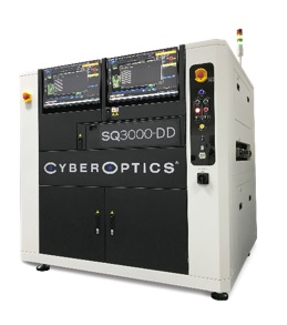
CyberOptics Corporation will demonstrate the SQ3000-DD 3D automated optical inspection (AOI) system with the new ultra-high resolution multiple-reflection suppression (MRS) sensors in hall A4, stand 239 at productronica 2017, scheduled to take place November 14 – 17, 2017 at the Messe Munchen in Germany. The company also will unveil the new SE3000 3D SPI and SQ3000 3D CMM, both powered by MRS technology.
The new SQ3000-DD 3D AOI dual lane, dual sensor system maximizes flexibility catering to varying PCB widths. This unique design provides the ability to inspect high volume assemblies, the convenience of inspecting different assemblies and board sizes simultaneously on different lanes, or even switching from dual lane to single lane mode to inspect very large boards.
Not only does the SQ3000-DD provide the PCB inspection flexibility, it also provides the flexibility to choose two of the same or two different proprietary MRS sensors, both of which meticulously identify and reject multiple reflections caused by shiny components and reflective solder joints.
The new ultra-high-resolution MRS sensor option provides an even finer resolution than the standard, delivering superior inspection performance ideally suited for 0201 metric and microelectronics applications where an even greater degree of accuracy and inspection reliability is critical. The unique architecture of both MRS sensor options simultaneously captures and transmits multiple images in parallel, while highly sophisticated 3D fusing algorithms merge the images together, delivering microscopic image quality at production speed.
The new SE3000 SPI system is the very first SPI system to incorporate the industry-leading MRS sensor technology with a finer resolution for the best accuracy, repeatability and reproducibility – even on the smallest paste deposits. Combined with the award-winning, easy-to-use software, solder paste inspection has reached a new level of precision for the most stringent requirements.
“We’ve incorporated our MRS sensor technology into multiple platforms for AOI, SPI and CMM,” said Dr. Subodh Kulkarni, President and CEO, CyberOptics, “Providing our customers with the best combination of accuracy, speed and ease-of-use to maximize their yields and productivity.”
The new SQ3000 3D CMM (Coordinate Measurement) system, powered by Multi-Reflection Suppression (MRS) technology utilizes CyberCMM, a new comprehensive software suite for coordinate measurement. In a lab or production environment, the MRS-enabled SQ3000 CMM system is extremely fast and highly accurate, with repeatable and reproducible measurements for metrology applications in manufacturing of a wide variety of products such as PCBs, semiconductors and consumer electronics.
CyberCMM, an extensive suite of CMM tools, provides 100 percent metrology-grade measurement on all critical points much faster than a traditional CMM, including coplanarity, distance, height and datum X, Y, to name a few. A fast and easy setup can be performed as compared to a slow, engineering resource-intensive setup that typically requires multiple adjustments with traditional CMMs.
About CyberOptics
CyberOptics Corporation is a leading global developer and manufacturer of high precision sensing technology solutions. CyberOptics sensors are being used in general purpose metrology and 3D scanning, surface mount technology (SMT) and semiconductor markets to significantly improve yields and productivity. By leveraging its leading-edge technologies, the company has strategically established itself as a global leader in high precision 3D sensors, allowing CyberOptics to further increase its penetration of its key vertical markets. Headquartered in Minneapolis, Minnesota, CyberOptics conducts worldwide operations through its facilities in North America, Asia and Europe.
For more information, click here.


