


 Flexible Thinking: Designing Flex Circuits for Dynamic Reliability
 Global PCB Connections: Rigid-flex and Flexible PCBs—The Backbone of Modern Electronics
 Happy’s Tech Talk #29: Bend-to-Install Semi-flex FR-4


Being a new person in any industry comes with a sharp learning curve. Gaining the necessary knowledge, experience, and skill can come from a variety of sources, such as specific training, attending industry events and trade shows, and experiential learning.
Recently, Anaya Vardya, CEO of American Standard Circuits, invited two of I-Connect007’s newest team members, IT Coordinator Jonathan Zinski and Editor Kiersten Rohde, to tour his facility in West Chicago, Illinois. Happy Holden, resident PCB expert, also joined the newbies on their field trip to ASC.
In the following articles, Jonathan and Kiersten describe their experience touring ASC. Special thanks to Anaya for hosting the I-Connect007 team.
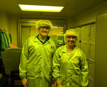
Only the Beginning
by Kiersten Rohde, I-Connect007
Most end-users don't consider the internal components of the devices they use every day. These household devices might include cellphones, computers, microwaves, or even toasters. As a millennial who is new to the industry (and in a non-technical role as an editor for I-Connect007), I have most often experienced the end-products. Little did I realize that inside many of these devices were PCBs—the detailed and fundamental part that serves as the foundation for electronic devices.
My appreciation for the PCB industry expanded when I had the opportunity to tour American Standard Circuits’ facility in West Chicago, Illinois. CEO Anaya Vardya guided me and Jonathan, another millennial coworker, through a number of different process steps involved in making a PCB. We learned more than we could have imagined about PCB construction, and at times were slightly overwhelmed with all the new information.
Throughout the tour, I learned that ASC produces PCBs for much more than typical household uses; they also handle PCB construction for other crucial areas, such as medical and military/aerospace. Further, seeing PCBs being built made some of the terms I’ve encountered “come to life” by connecting them to real materials, factors, components, processes, and applications.
Moving from the very early steps of creating a PCB, we explored various rooms, such as the warehouse, drill room, and yellow room where we wore bunny suits (no, not for Halloween) for entering the cleanroom. During the tour, it quickly became clear that there are numerous steps involved in constructing a PCB, and these steps must be meticulously executed. Employees often handle boards multiple times to successfully finish the PCBs and send them to customers without any errors.
Because I’m a detail-oriented person, I most enjoyed learning about the necessary quality inspection tests done to ensure the final PCBs meet IPC standards. Who would have guessed it, especially since I’m an editor! I was impressed by AOI technology used to identify anomalies on the inner layers and outer layers and correct them when possible. Additionally, seeing a cross-section of a board examined under a microscope to measure copper thickness in the vias using computer software also amazed me.
Overall, I didn’t know what to expect when we stepped out of our Lyft ride at the front doors of American Standard Circuits, but I left with an increased knowledge base that I can continue to build. What I experienced will help me to better understand the content I read and edit and to view the various technical components as less conceptual and more concrete. Although I'm only beginning to learn about how PCBs are made and how they operate, I now know how integral PCBs are to electronics of all kinds. I hope this is only the beginning of my growth in the industry.
Page 1 of 2


