


 Trouble in Your Tank: Implementing Direct Metallization in Advanced Substrate Packaging
 It’s Only Common Sense: Storytelling That Sells—Stop Pitching, Start Painting Pictures
 The Right Approach: Get Ready for ISO 9001 Version 6


Hybrid Circuit Combines Single-Photon Generator and Efficient Waveguides on One Chip
November 8, 2017 | NISTEstimated reading time: 4 minutes
Scientists at the National Institute of Standards and Technology (NIST) and their collaborators have taken a new step forward in the quest to build quantum photonic circuits—chip-based devices that rely on the quantum properties of light to process and communicate information rapidly and securely.
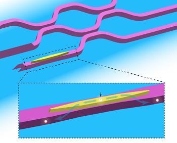
The quantum circuit architecture devised by the team is among the first to combine two different types of optical devices, made from different materials, on a single chip—a semiconductor source that efficiently generates single particles of light (photons) on demand, and a network of “waveguides” that transports those photons across the circuit with low loss. Maximizing the number of photons, ideally having identical properties, is critical to enabling applications such as secure communication, precision measurement, sensing and computation, with potentially greater performance than that of existing technologies.
The architecture, developed by Marcelo Davanco and other NIST researchers along with collaborators from China and the U.K., employs a nanometer-scale semiconductor structure called a quantum dot—made from indium arsenide—to generate individual photons on the same chip as the optical waveguides—made from silicon nitride. Combining these two materials requires special processing techniques. Such hybrid circuit architectures could become building blocks for more complex systems.
Previously, quantum integrated photonic circuits typically consisted of only passive devices such as waveguides and beam splitters, which let photons through or allowed them to coalesce. The photons themselves still had to be produced outside the chip, and getting them onto the chip resulted in losses, which significantly degraded the performance of the circuit. Circuit architectures that did include quantum light generation on a chip either incorporated sources that only produced photons randomly and at low rates—which limits performance—or had sources in which one photon was not necessarily identical with the next. In addition, the fabrication processes supporting these previous architectures made it difficult to scale up the number, size and complexity of the photonic circuits.
In contrast, the new architecture and the fabrication processes the team developed should enable researchers to reliably build larger circuits, which could perform more complex computations or simulations and translate into higher measurement precision and detection sensitivity in other applications.
The quantum dot employed by the team is a well-studied nanometer-scale structure: an island of the semiconductor indium arsenide surrounded by gallium arsenide. The indium arsenide/gallium arsenide nanostructure acts as a quantum system with two energy levels—a ground state (lower energy level) and an excited state (higher energy level). When an electron in the excited state loses energy by dropping down to the ground state, it emits a single photon.
Unlike most types of two-level emitters that exist in the solid state, these quantum dots have been shown to generate—reliably, on demand, and at large rates—the single photons needed for quantum applications. In addition, researchers have been able to place them inside nanoscale, light-confining spaces that allow a large speedup of the single-photon emission rate, and in principle, could also allow the quantum dot to be excited by a single photon. This enables the quantum dots to directly assist with the processing of information rather than simply produce streams of photons.
The other part of the team’s hybrid circuit architecture consists of passive waveguides made of silicon nitride, known for their ability to transmit photons across a chip’s surface with very low photon loss. This allows quantum-dot-generated photons to efficiently coalesce with other photons at a beam splitter, or interact with other circuit elements such as modulators and detectors.
“We’re getting the best of both worlds, with each behaving really well together on a single circuit,” said Davanco. In fact, the hybrid architecture keeps the high performance achieved in devices made exclusively of each of the two materials, with little degradation when they are put together. He and his colleagues described the work (link is external) in a recent issue of Nature Communications.
To make the hybrid devices, Davanco and his colleagues first bonded two wafers together—one containing the quantum dots, the other containing the silicon nitride waveguide material. They used a variation of a process that had originally been developed for making hybrid photonic lasers, which combined silicon for waveguides and compound semiconductors for classical light emission. Once the bonding was finished, the two materials were then sculpted with nanometer-scale resolution into their final geometries through state-of-the-art semiconductor device patterning and etching techniques.
Although this wafer bonding technique was developed more than a decade ago by other researchers, the team is the first to apply it towards making integrated quantum photonic devices.
“Since we have expertise in both fabrication and quantum photonics, it seemed clear that we could borrow and adapt this process to create this new architecture,” notes Davanco.
This work was performed in part at NIST's Center for Nanoscale Science and Technology (CNST), a shared-use facility available to researchers from industry, academia and government, and also included researchers from NIST’s Physical Measurement Laboratory.
Share on:


Testimonial
"The I-Connect007 team is outstanding—kind, responsive, and a true marketing partner. Their design team created fresh, eye-catching ads, and their editorial support polished our content to let our brand shine. Thank you all! "
Sweeney Ng - CEE PCBSuggested Items
Indium to Highlight Energy-Efficient, High-Reliability Solder Solutions for EV and Electronics at Productronica India
09/03/2025 | Indium CorporationIndium Corporation, a leading materials refiner, smelter, manufacturer, and supplier to the global electronics, semiconductor, electric vehicle (EV), thin-film, and thermal management markets, will feature a range of sustainable, high-reliability solder products at Productronica India, to be held September 17-19 in Bengaluru, India.
Indium Promotes Huang to Senior Manager, Marketing Communications
08/28/2025 | Indium CorporationWith its commitment to innovation and growth through employee development, Indium Corporation announces the promotion of Jingya Huang to Senior Manager, Marketing Communications, to continue to lead the company’s branding and promotional efforts.
Indium Expert to Present on AI Thermal Challenges at INEMI Forum on Complex Integrated Electronics
08/26/2025 | Indium CorporationIndium Corporation Assistant Product Manager Foo Siang Hooi will deliver a technical presentation on addressing thermal challenges in AI and high-performance computing (HPC) with metal-based thermal interface materials (TIMs) at the International Electronics Manufacturing Initiative (INEMI) Forum on Complex Integrated Electronics, to be held September 17-18 in Penang, Malaysia.
Indium Corporation to Showcase Innovative Materials Enabling AI Technology at SEMICON Taiwan
08/20/2025 | Indium CorporationIndium Corporation®, a leading materials refiner, smelter, manufacturer, and supplier to the global electronics, semiconductor, AI, thin-film, and thermal management markets, will showcase its heterogeneous integration and assembly (HIA) products and thermal interface materials (TIMs) at SEMICON Taiwan, to be held September 10-12 in Taipei, Taiwan.
Indium Corporation Promotes Two Leaders in EMEA (Europe, Middle East, and Africa) Markets
08/05/2025 | Indium CorporationWith its commitment to innovation and growth through employee development, Indium Corporation today announced the promotions of Andy Seager to Associate Director, Continental Sales (EMEA), and Karthik Vijay to Senior Technical Manager (EMEA). These advancements reflect their contributions to the company’s continued innovative efforts with customers across Europe, the Middle East, and Africa (EMEA).