


 Standard of Excellence: The Future of Fabrication—From Art to Automation
 Knocking Down the Bone Pile: The Business Case for Component Reclamation
 Global Sourcing Spotlight: The Hidden Power of the Rep Network


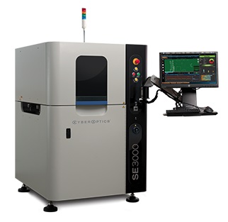
CyberOptics will demonstrate the new SE3000 3D Solder Paste Inspection (SPI) system with a proprietary Multiple-Reflection Suppression (MRS) Sensor in Hall A2, Stand 439 at productronica 2017, taking place November 14-17, 2017 at the Messe München, in Germany.
SE3000The new SE3000 3D SPI system is the very first SPI system to incorporate the industry-leading MRS sensor technology, with a finer resolution for the best accuracy, repeatability and reproducibility – even on the smallest paste deposits. The unique sensor architecture simultaneously captures and transmits multiple images in parallel, while highly sophisticated 3D fusing algorithms merge the images together, delivering microscopic image quality at production speed. Combined with the award-winning, easy-to-use software, solder paste inspection has reached a new level of precision for the most stringent requirements.
“Smaller and mobile is a key trend driving the demand for an even higher level of accuracy and resolution,” said Dr. Subodh Kulkarni, President and CEO, CyberOptics, “We’ve optimized our proprietary MRS sensor technology that is widely used for Automated Optical Inspection applications world-wide, and integrated it into our new SE3000 SPI system to address these critical customer requirements better than any alternate solution.”
For maximum flexibility, the new SE3000-DD 3D AOI dual lane, dual sensor system caters to varying widths. This unique design provides the ability to inspect high volumes, the convenience of inspecting different board sizes simultaneously on different lanes, or even switching from dual lane to single lane mode to inspect very large boards.
At productronica Germany, CyberOptics will also unveil the new SQ3000 3D CMM system and the new SQ3000-DD™ 3D AOI system, both powered by MRS technology.


