


 Dan’s Biz Bookshelf: ‘Believe in Better'
 The Big Picture: Our Big ‘Why’ in the Age of AI
 The Chemical Connection: Through-glass Vias in Glass Substrates


Orbotech Gets $31M Worth of Orders from Leading Japanese Electronics Components Manufacturer
November 14, 2017 | OrbotechEstimated reading time: 3 minutes
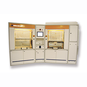
Orbotech Ltd. announced today that it has received orders totaling $31 million for a variety of solutions from a leading Japanese electronics components manufacturer. The manufacturer, a long-time Orbotech partner with facilities located worldwide, selected Orbotech’s Direct Imaging (DI), Inkjet and Automated Optical Inspection (AOI) PCB production solutions, as part of its program to expand the capacity of its multilayer flex component manufacturing lines for organic material components of the latest generation of smartphones.
“We have seen consistent growth in our smartphone business in both volume and in increasingly advanced features,” said the VP of the Manufacturing and Engineering Unit of the leading Japanese electronics components manufacturer. “As the processes supporting these features become more complex, Orbotech’s advanced technologies help us to keep our competitive advantage while expanding our capacity.”
“We are proud to enable our customers to maintain their technological edge with our advanced solutions,” said Yair Alcobi, President of Orbotech PCB South East Asia. “Our close collaborations with leading manufacturers worldwide allow us to develop solutions that improve our customers’ capabilities and enable the industry to move forward.”
Solutions ordered include the Paragon Ultra, delivering superior Direct Imaging (DI) accuracy and yields for the industry’s most complex IC substrates, and the Nuvogo 1000 for large-format DI, enabling consistent high-quality DI for both patterning and solder mask at unmatched throughput and quality. The deal also included Sprint 200 Flex for inkjet printing and the Ultra Fusion 200 AOI (Automated Optical Inspection) solution. Delivery of all orders is expected to be completed in 2018.
About Paragon Ultra S R2R
Featuring the leading-edge performance of Orbotech’s Large Scan Optics (LSO) Technology, Paragon Ultra Laser Direct Imaging (LDI) solutions deliver the highest imaging accuracy and throughput for HDI, Flex and Rigid-Flex applications and today’s most complex IC substrate applications, including Flip-Chip BGA, Flip-Chip CSP, BGA/CSP and modules manufacturing. The Paragon Ultra line provides high throughput using enhanced electronics and a powerful laser system and provides exceptional results on both conventional UV and LDI resists.
About Nuvogo 1000
Nuvogo 1000 is a member of the Orbotech’s Nuvogo series of industry-leading Direct Imaging (DI) solutions. Utilizing a high-power laser and unique MultiWave Laser Technology, the Nuvogo 1000 provides maximum flexibility on a wide range of materials and applications. Incorporating Orbotech’s field-proven Large Scan Optics (LSO) Technology with its high depth-of-focus, the Nuvogo 1000 is a perfect match for flex patterning and solder mask applications that demand fine structures on variating topography. This powerful solution is designed for high throughput while maintaining optimal quality.
About Sprint 200 Flex
The Sprint 200 Flex Inkjet Printer is Orbotech’s mass production, digital legend inkjet printing solution, optimized for flex multi-panel PCB production. This latest addition to Orbotech’s series of high performance PCB legend inkjet printers delivers cost-effective, top quality, industrial inkjet printing for a consistently accurate production of even the most complex legend designs. The Sprint 200 Flex offers manufacturers breakthrough performance for high volume, high yield and high quality legend and serialization printing over a range of flex PCB materials.
About Ultra Fusion 200
Ultra Fusion 200 delivers leading-edge AOI (Automated Optical Inspection) performance for SLP/mSAP, advanced HDI, flex & ICS applications down to 15µm L/S. Featuring powerful Multi-Image Technology™, the system improves process efficiency by reducing the rate of false alarms up to 70% compared with conventional AOI.
About Orbotech Ltd.
Orbotech Ltd. is a leading global supplier of yield-enhancing and process-enabling solutions for the manufacture of electronics products. Orbotech provides cutting-edge solutions for use in the manufacture of printed circuit boards (PCBs), flat panel displays (FPDs), and semiconductor devices (SDs), designed to enable the production of innovative, next-generation electronic products and improve the cost effectiveness of existing and future electronics production processes. Orbotech’s core business lies in enabling electronic device manufacturers to inspect and understand PCBs and FPDs and to verify their quality (‘reading’); pattern the desired electronic circuitry on the relevant substrate and perform three-dimensional shaping of metalized circuits on multiple surfaces (‘writing’); and utilize advanced vacuum deposition and etching processes in SD and semiconductor manufacturing (‘connecting’). Orbotech refers to this ‘reading’, ‘writing’ and ‘connecting’ as enabling the ‘Language of Electronics’. For more information, visit www.orbotech.com and www.spts.com.
Share on:


Suggested Items
Indium Corporation Expert to Present on Automotive and Industrial Solder Bonding Solutions at Global Electronics Association Workshop
06/26/2025 | IndiumIndium Corporation Principal Engineer, Advanced Materials, Andy Mackie, Ph.D., MSc, will deliver a technical presentation on innovative solder bonding solutions for automotive and industrial applications at the Global Electronics A
Fresh PCB Concepts: Assembly Challenges with Micro Components and Standard Solder Mask Practices
06/26/2025 | Team NCAB -- Column: Fresh PCB ConceptsMicro components have redefined what is possible in PCB design. With package sizes like 01005 and 0201 becoming more common in high-density layouts, designers are now expected to pack more performance into smaller spaces than ever before. While these advancements support miniaturization and functionality, they introduce new assembly challenges, particularly with traditional solder mask and legend application processes.
Knocking Down the Bone Pile: Tin Whisker Mitigation in Aerospace Applications, Part 3
06/25/2025 | Nash Bell -- Column: Knocking Down the Bone PileTin whiskers are slender, hair-like metallic growths that can develop on the surface of tin-plated electronic components. Typically measuring a few micrometers in diameter and growing several millimeters in length, they form through an electrochemical process influenced by environmental factors such as temperature variations, mechanical or compressive stress, and the aging of solder alloys.
SolderKing’s Successful Approach to Modern Soldering Needs
06/18/2025 | Nolan Johnson, I-Connect007Chris Ward, co-founder of the family-owned SolderKing, discusses his company's rapid growth and recent recognition with the King’s Award for Enterprise. Chris shares how SolderKing has achieved these award-winning levels of service in such a short timeframe. Their secret? Being flexible in a changing market, technical prowess, and strong customer support.
Preventing Surface Prep Defects and Ensuring Reliability
06/10/2025 | Marcy LaRont, PCB007 MagazineIn printed circuit board (PCB) fabrication, surface preparation is a critical process that ensures strong adhesion, reliable plating, and long-term product performance. Without proper surface treatment, manufacturers may encounter defects such as delamination, poor solder mask adhesion, and plating failures. This article examines key surface preparation techniques, common defects resulting from improper processes, and real-world case studies that illustrate best practices.