


 Powering the Future: When Material Choice Defines RF Performance
 Learning with Leo: The Cost of Cleaning and Protecting the Ozone Layer
 Nolan’s Notes: Cleaning With Smaller Geometries


There is a growing trend towards the use of HDI in electronics manufacturing. A simple reason is that people want greater performance from their electronics, now more than ever. From an electronics design standpoint, greater performance means more switches or transistors. More transistors mean more power. Counterintuitively, more power requirements of a device means you need to lower the power of the whole system or subassembly. You also need to lower the power because then, you need to deal with thermal management.
To lower the power requirement, everything must be reduced. As such, the components keep getting smaller and smaller. Pin pitches are now down to 0.25 mm or around 10 mil. On top of that, the overall density of board assemblies continuously increases in line with the growing demand for more features and functions. Adding to that challenge is the shrinking PCB real estate on which to put this increasing number of components.
Our recent survey on HDI found that the three key factors driving HDI work are: overall density, fine pitch of components, and the high pin counts of ICs (Chart 1).
At present, majority of our surveyed respondents say up to 25% of PCBs they work with use HDI technology (Chart 2).
In three years, nearly half of the respondents answered that HDI technology will account for at least 50% of their PCB work. This is across a variety of industries, top three of which are consumer electronics, telecommunications, and automotive electronics. In particular, the emergence of 5G and Internet of Things (IoT) are expected to bolster the use of HDI technology due to frequency and signaling requirements (Chart 3).
Assemblers have different areas of concern regarding HDI than fabricators and designers. When it comes down to having vias in the boards, especially vias in pads, issues will arise if the assembly is the not done properly. "When you put a via in a pad, you typically want to fill that via, with either a non-conductive or conductive epoxy, and use some sort of plating over the barrel of the via so that you get a smooth pad that you are assembling the part to without a whole lot of surface deviation. The flatter the pad, the easier it is to print solder on the board, and to assemble the part," said Garret Maxson of EMS firm ACDi.
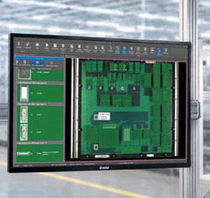
This month’s issue of SMT Magazine examines the challenges when dealing with HDI from an assembly perspective. We start with a roundtable between HDI experts Steve Bird of Finisar, Tony Torres of APCT, and technologists from EMS firm MC Assembly, including Vince Burns, Steve Jervey, Mike Smyth, and Paul Petty. The discussion covers the latest technology developments, manufacturing challenges, and HDI strategies, from the design, fabrication, and assembly perspectives. What we found out is that, while there may be new techniques and strategies, technologies, equipment, tools, and materials to employ and utilize, there is always one thing that will ensure the manufacturing/ assembly success of your product: communication.
Communication between the designer and the assembler will help improve the manufacturability and assembly of the final product—even before the board design gets fabricated. As Vince Burns of MC Assembly says, "It's not just designing the perfect circuit, but it has to be manufacturable, and that’s where our input comes in."
There is value to be added in collaborating with the designers in the very first stages of the design. Indeed, the goal is working together as a team and sharing the expertise of one another to make sure that the design is manufacturable, and the final product is of high quality and reliable.
To read the full version of this article, which appeared in the November 2017 issue of SMT Magazine, click here.


