


 Dan’s Biz Bookshelf: ‘Believe in Better'
 The Big Picture: Our Big ‘Why’ in the Age of AI
 The Chemical Connection: Through-glass Vias in Glass Substrates


Ventec International Launches Latest Mobile tec-APP
December 14, 2017 | Ventec International GroupEstimated reading time: Less than a minute
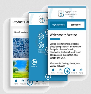
Ventec International Group, a world leader in the production of insulated metal substrates, thermally conductive polyimide & high reliability laminates and prepregs, is pleased to announce the launch of its latest mobile tec-APP available through the App Store (IOS) and Google Play for Android.
The Ventec mobile tec-APP has had a complete facelift giving direct access to all technical updates and news at the touch of a button. With an improved and intuitive user-interface, the app provides up-to-the-minute information on all developments, technical data updates, ongoing projects and news from Ventec's operations across the world including the latest data sheets and process guidelines. The Ventec app is completely free to download and is compatible with all Apple and Android devices.
About Ventec International Group
With volume manufacturing facilities and HQ in Suzhou China, Ventec International specializes in advanced copper clad glass reinforced and metal backed substrates for the PCB industry. With distribution locations and manufacturing sites in both the US and Europe, Ventec International is a premier supplier to the Global PCB industry.
For more information, click here.
Share on:


Suggested Items
The Evolution of Picosecond Laser Drilling
06/19/2025 | Marcy LaRont, PCB007 MagazineIs it hard to imagine a single laser pulse reduced not only from nanoseconds to picoseconds in its pulse duration, but even to femtoseconds? Well, buckle up because it seems we are there. In this interview, Dr. Stefan Rung, technical director of laser machines at Schmoll Maschinen GmbH, traces the technology trajectory of the laser drill from the CO2 laser to cutting-edge picosecond and hybrid laser drilling systems, highlighting the benefits and limitations of each method, and demonstrating how laser innovations are shaping the future of PCB fabrication.
Day 2: More Cutting-edge Insights at the EIPC Summer Conference
06/18/2025 | Pete Starkey, I-Connect007The European Institute for the PCB Community (EIPC) summer conference took place this year in Edinburgh, Scotland, June 3-4. This is the third of three articles on the conference. The other two cover Day 1’s sessions and the opening keynote speech. Below is a recap of the second day’s sessions.
Day 1: Cutting Edge Insights at the EIPC Summer Conference
06/17/2025 | Pete Starkey, I-Connect007The European Institute for the PCB Community (EIPC) Summer Conference took place this year in Edinburgh, Scotland, June 3-4. This is the second of three articles on the conference. The other two cover the keynote speeches and Day 2 of the technical conference. Below is a recap of the first day’s sessions.
Preventing Surface Prep Defects and Ensuring Reliability
06/10/2025 | Marcy LaRont, PCB007 MagazineIn printed circuit board (PCB) fabrication, surface preparation is a critical process that ensures strong adhesion, reliable plating, and long-term product performance. Without proper surface treatment, manufacturers may encounter defects such as delamination, poor solder mask adhesion, and plating failures. This article examines key surface preparation techniques, common defects resulting from improper processes, and real-world case studies that illustrate best practices.
RF PCB Design Tips and Tricks
05/08/2025 | Cherie Litson, EPTAC MIT CID/CID+There are many great books, videos, and information online about designing PCBs for RF circuits. A few of my favorite RF sources are Hans Rosenberg, Stephen Chavez, and Rick Hartley, but there are many more. These PCB design engineers have a very good perspective on what it takes to take an RF design from schematic concept to PCB layout.