


 Dan’s Biz Bookshelf: ‘Abundance: How We Build a Better Future’
 Trouble in Your Tank: In Complex Systems, Design Rules Aren’t Optional
 It’s Only Common Sense: The Phone Is Still Your Competitive Advantage


Ventec Highlights Advanced Ultra-Low Dk PCB Materials at DesignCon 2018
January 8, 2018 | Ventec InternationalEstimated reading time: 2 minutes
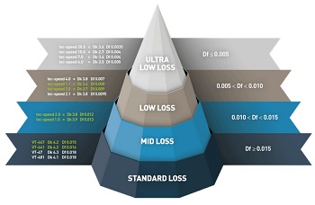
Ventec International will showcase its extensive range of tec-speed materials for high-speed low-loss applications including the latest tec-speed 10 ultra-low dk material at DesignCon 2018 show in Santa Clara, California, USA from 30 January to 1 February in booth #118. A further highlight will be a next generation best-in-class, thermally conductive (8 X FR-4) high Tg thin-core and prepreg material (VT-5A2) ideal for hybrid multilayer low-loss constructions.
Ventec will be exhibiting at DesignCon 2018, the premier conference for chip, board, and systems design engineers, on booth #118 highlighting it’s tec-speed range of PCB materials for high-speed low-loss applications. By using an ultra-low Dk material with Dk values between 2.3 and 2.8 lower losses, lower system power requirements and with it the delicate balance of performance and cost can be achieved. Higher layer counts on backplanes, daughter cards and hand-held's are made possible in a smaller footprint by having smaller layer to layer separation without sacrificing trace width.
“Maintaining wider traces produces lower resistance in the signal path," said Martin Cotton, Director of OEM Technology Marketing. "Combining ultra-low Dk with a low Df of 0.003 to 0.004, produces an alternative to ever smaller traces and higher power requirements."
Ventec’s highest performance thermally conductive laminate material so far will also make its DesignCon debut. VT-5A2 offers a polymer matrix that is fully compatible with Ventec laminates, epoxy or polyimide based materials including tec-speed, making it the ideal choice for the manufacture of hybrid multilayer low-loss constructions.
Cotton and Peter Koolen, Global Account Manager for OEM Technology Marketing, will be on hand to offer technical advice.
About Ventec International
With volume manufacturing facilities and HQ in Suzhou China, Ventec International specializes in advanced copper clad glass reinforced and metal backed substrates for the PCB industry. With distribution locations and manufacturing sites in both the US and Europe, Ventec International is a premier supplier to the Global PCB industry. For more information, click here.
Share on:


Testimonial
"The I-Connect007 team is outstanding—kind, responsive, and a true marketing partner. Their design team created fresh, eye-catching ads, and their editorial support polished our content to let our brand shine. Thank you all! "
Sweeney Ng - CEE PCBSuggested Items
Driving Innovation: Selecting the Right Laser Source
04/28/2026 | Simon Khesin -- Column: Driving InnovationWhen I first joined Schmoll Maschinen, I brought experience from almost every PCB process, except for laser. As I immersed myself in laser processing, I realized why it can seem so daunting to a newcomer. The complexity arises from three intersecting factors: A vast variety of laser sources: CO2, UV-nano, green-pico, UV-pico, IR-pico, and others; a diverse range of applications: Drilling, cutting, ablation, and more; and an extensive list of materials: These have vastly different absorption rates. Choosing the right machine or laser source is rarely trivial. Even for experienced engineers, answering "Which source is best?" requires examining the business's specific goals.
Institute of Circuit Technology Spring Seminar 2026: A Bright Future in Europe
04/23/2026 | Pete Starkey, I-Connect007Through the leafy lanes and spring flowers of Warwickshire and back to Meridan, the traditional centre of England, and now officially part of the Metropolitan Borough of Solihull in the county of the West Midlands, I attended the Annual General Meeting and Spring Seminar of the Institute of Circuit Technology (ICT) on April 14. Out of the AGM came notable changes in leadership at the top of the Institute: the retirement of Mat Beadel as chair and Emma Hudson as technical director. Effective May 1, Steve Driver is the new chair, and Alun Morgan is the new technical director.
ACCM Unveils Negative and Near-zero CTE Materials for Large-Format AI Chips
04/21/2026 | Advanced Chip and Circuit MaterialsAdvanced Chip and Circuit Materials, Inc. (ACCM) has launched two new materials: Celeritas HM50, with a negative coefficient of thermal expansion (CTE) of -8 ppm/°C to offset the positive CTE and expansion of copper with temperature on circuit boards, and Celeritas HM001, with near-zero CTE and the low-loss performance needed for high-speed signal layers to 224 Gb/s and faster in artificial intelligence (AI) circuits.
Fresh PCB Concepts: Designing PCBs for Harsh Environments—Reliability Is Engineered Upstream
04/23/2026 | Team NCAB -- Column: Fresh PCB ConceptsWhen engineers hear the phrase “harsh environment,” they usually think of the extreme temperature swings, vibration and shock, pressure changes, or radiation in aerospace. However, aerospace is not the only harsh environment where electronic assemblies must survive. Automotive power electronics, downhole oil and gas tools, marine controls, rail systems, defense platforms, and industrial automation equipment all expose PCBs to environments that are equally unforgiving. The stress mechanisms may differ, but the physics does not.
Advanced Packaging for AI: Reliability Starts at the Cu/Cu/Cu Microvia Junction
04/20/2026 | Kuldip Johal, MKS' AtotechThe rapid growth of AI computing, from training clusters to inference at scale, is reshaping demand across the entire electronics supply chain. Advances in technology requirements, such as higher bandwidth, lower latency, and greater compute density, are driving the development of advanced packaging technologies and transforming the PCB industry across design, manufacturing, testing, and even architecture.