


 Trouble in Your Tank: Implementing Direct Metallization in Advanced Substrate Packaging
 It’s Only Common Sense: Storytelling That Sells—Stop Pitching, Start Painting Pictures
 The Right Approach: Get Ready for ISO 9001 Version 6


First 3-D Imaging of Excited Quantum Dots
February 9, 2018 | AIP.orgEstimated reading time: 2 minutes
Quantum dots are rapidly taking center stage in emerging applications and research developments, from enhanced LCD TVs and thin-film solar cells, to high-speed data transfer and fluorescent labeling in biomedical applications.
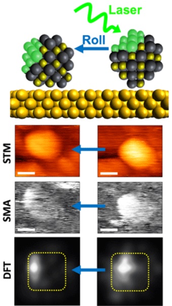
Image caption:
Top: Side-view image of a quantum dot with a defect excited by a laser (green) rolled to present a different orientation.
STM: Conventional STM image of a quantum dot before (right) and after a roll (left).
SMA: Slice through the electronic density of the excited quantum dot before and after the same roll.
DFT (density functional theory): 3-D quantum calculation of a quantum dot defect projected into slices at two orientations for comparison with experiment. Credit: Martin Gruebele
Researchers are still studying how to precisely control the growth of these nanoscale particles and their underlying quantum behavior. For instance, defects form during production of semiconductor materials, so identical dots can differ in composition from one another.
To learn more about these defects -- and whether they are a bane or an advantage -- a U.S. research team, from the University of Illinois and the University of Washington, has, for the first time, demonstrated imaging of an electronically excited quantum dot at multiple orientations. They report their findings this week in The Journal of Chemical Physics, from AIP Publishing.
“Understanding how the presence of defects localizes excited electronic states of quantum dots will help to advance the engineering of these nanoparticles,” said Martin Gruebele from the University of Illinois at Urbana-Champaign and a co-author of the paper.
Defects are often considered a hassle, but in the case of quantum dot applications, they are purposely created by doping any number of materials to impart specific functions. “[M]issing atoms in a quantum dot or substituting a different kind of atom are defects that will alter the electronic structure and change the semiconductivity, catalysis or other nanoparticle properties,” Gruebele said. “If we can learn to characterize them better and precisely control how they are produced, defects will become desirable dopants instead of a nuisance.”
In 2005, Gruebele’s team created a new imaging technique, called single molecule absorption scanning tunneling microscopy (SMA-STM), that combines the high spatial resolution of a scanning tunneling microscope with the spectral resolution of a laser. SMA-STM allows individual nanoparticles to be imaged in a laser beam, so their excited electronic structure can be visualized.
Using the thin, sharp metal wire tip of the scanning tunneling microscope, they roll the laser-excited quantum dot on the surface to image slices at different orientations. The slices can be combined to reconstruct a 3-D image of an electronically excited quantum dot.
While the research in this article was limited to lead sulfide and cadmium selenide/zinc sulfide quantum dots, the technique can potentially be expanded to other compositions. Furthermore, SMA-STM can also be used to explore other nanostructures, such as carbon nanotubes and photocatalytic metal clusters.
Researchers are now working to advance SMA-STM into a single-particle tomography technique. But, before SMA-STM becomes a “true single-particle tomography approach,” they still have to ensure that the scanning and rolling does not damage the nanoparticle while it is being reoriented.
“We speculate that, in the future, it may be possible to do single-particle tomography if damage to quantum dots can be avoided during repeated manipulation,” Gruebele said.
Single-particle tomography would provide a clearer picture than conventional tomography by singling out defects in individual nanoparticles rather than re-creating an averaged 3-D image that combines the measurements of many particles.
Share on:


Testimonial
"Our marketing partnership with I-Connect007 is already delivering. Just a day after our press release went live, we received a direct inquiry about our updated products!"
Rachael Temple - AlltematedSuggested Items
TRI to Unveil New High-Throughput AOI and AXI at productronica 2023
09/15/2023 | TRITest Research, Inc. (TRI), the leading test and inspection systems provider for the electronics manufacturing industry, will join productronica 2023, which will be held at Messe München Center from November 14 – 17, 2023.
UK Space Agency Launches Consultation on Variable Liability Limits for Orbital Operations
09/15/2023 | UK Space AgencyThe proposals from the UK Space Agency follow a review into the UK’s approach to setting the amount of an operator’s liability in licences for orbital operations, a key commitment of the government’s National Space Strategy.
MediaTek Successfully Develops First Chip Using TSMC's 3nm Process, Set for Volume Production in 2024
09/14/2023 | MediaTekMediaTek and TSMC announced that MediaTek has successfully developed its first chip using TSMC's leading-edge 3nm technology, taping out MediaTek’s flagship Dimensity system-on-chip (SoC) with volume production expected next year.
MKS’ Atotech to Participate in IPCA Expo 2023
09/14/2023 | MKS’ AtotechMKS’ Atotech, a leading surface finishing brand of MKS Instruments, will participate in the upcoming IPCA Expo at Bangalore International Exhibition Centre (BIEC) and showcase its latest PCB manufacturing solutions from September 13 – 15.
Comtech Unveils New BRIDGE Solutions to Increase Access to Global Hybrid Connectivity
09/12/2023 | Business WireComtech launched its new blended, resilient, integrated, digital, global, end-to-end (BRIDGE) connectivity solutions. Comtech’s BRIDGE solutions provide portable, adaptable, full-service communications networks that can be established in a matter of hours and help “bridge the gap” for traditional satellite and terrestrial infrastructures.