














 The Big Picture: Not One, But Three Grey Rhinos
 It’s Only Common Sense: Make Your ‘Account’ the Whole Organization
 Dan’s Biz Bookshelf: ‘Building a Story Brand 2.0’





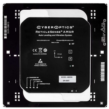
CyberOptics announces it will demonstrate its ReticleSense Auto Multi Sensors – efficient and effective wireless measurement devices for semiconductor fabs and equipment OEMs at SPIE Advanced Lithography at the San Jose Convention Center, February 27-28 at booth #314.
ReticleSense Auto Multi Sensors (AMSR) measure leveling, vibration, and relative humidity (RH) in an all-in-one wireless real-time device. The AMSR speeds equipment qualification, shorten equipment maintenance cycles and lower equipment maintenance expenses. Multiple measurements can be captured and monitored in all locations of the reticle environment, saving equipment engineers or process engineers’ time and expense.
CyberOptics will also demonstrate the ReticleSense Airborne Particle Sensor (APSRQ) that speeds equipment set-up and long-term yields in semiconductor fabs by wirelessly monitoring airborne particles in real-time. Engineers can save time by swiftly locating contamination sources and see the effect of cleanings, adjustments and repairs. In addition to small particles, the large particle detecting and measurement functionality covers a range of sizes with four bins for particles larger than 2, 5, 10 and 30 microns.
About the WaferSense and ReticleSense Line
The WaferSense measurement portfolio including the Auto Leveling System (ALS), the Auto Gapping System (AGS), the Auto Vibration System (AVS), the Auto Teaching System (ATS), the Airborne Particle Sensor (APS), the advanced Airborne Particle Sensors (APS2 and APS3) and the new Auto Multi Sensor (AMS) are available in various wafer shaped form factors depending on the device, including 150mm, 200mm and 300mm wafer sizes. The ReticleSense measurement portfolio including the Airborne Particle Sensor (APSR & APSRQ) and next-generation APS2, the Auto Leveling System (ALSR) and the Auto Multi Sensor (AMSR) are available in a reticle shaped form factor.
About CyberOptics
CyberOptics Corporation (NASDAQ: CYBE) is a leading global developer and manufacturer of high precision sensing technology solutions. CyberOptics sensors are being used in general purpose metrology and 3D scanning, surface mount technology (SMT) and semiconductor markets to significantly improve yields and productivity. By leveraging its leading edge technologies, the company has strategically established itself as a global leader in high precision 3D sensors, allowing CyberOptics to further increase its penetration of its key vertical segments. Headquartered in Minneapolis, Minnesota, CyberOptics conducts worldwide operations through its facilities in North America, Asia and Europe.
For more information about the entire line of CyberOptics solutions please click here.


