


 Global Sourcing Spotlight: Making Global Sourcing Simple Again
 The Government Circuit: New Council Now Helps Shape Policy Decisions in the Electronics Supply Chain
 Learning With Leo: Soldering—The Interpretation Problem


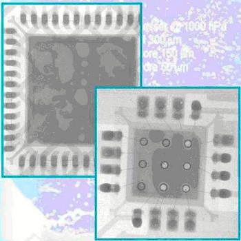
Requirements for void-free solder joints are continuously increasing in the field of electronics manufacturing, i.e. the reduction or elimination of cavities in the connection technology used between component connectors and connector pads. With its Void Expert database, Rehm is offering a tool which provides an overview of influencing factors and interaction amongst the mechanisms which result in voids.
The occurrence of voids is surely one of the most interesting phenomena associated with soft soldering. As a rule, larger or smaller voids can be found in most solder joints, which are formed as the result of gas which is trapped in the molten solder. When the molten solder hardens, these gas bubbles are frozen into place.
The reliability of most solder joints is not necessarily influenced decisively by voids contained within them, although there are exceptions. For example, sensitivity to voids is taking on new dimensions with regard to evolving package trends such as LGAs and QFNs. The greater the power loss which has to be dissipated via a solder joint, the lower its tolerability to voids is. In particular solder joints in power semiconductor devices should be nearly void-free.
This expert database makes a considerable contribution to understanding the mechanisms involved in the occurrence of voids and outgassing, and identifying the essential influencing variables. Influencing variables and the ways in which they interact are explained in a very clear-cut manner with reference to the respective response variables. Various graphics and Pareto charts help to clarify the interrelationships, which are quite complex in some cases. This allows the user to draw conclusions regarding how voids can be minimized for certain applications
The expert database developed by Dr. Heinz Wohlrabe from the Dresden Technical University presents results which are based on work conducted by the voids workgroup and knowledge gained through previous projects (in some cases subsidized projects), as well as the international literature. Experiments conducted to this end were evaluated by means of statistical methods.
The database is continuously updated with new findings and can be obtained from Rehm Thermal Systems.
About Rehm Thermal System
As a specialist in the field of thermal system solutions for the electronics and photovoltaics industries, Rehm is a technology and innovation leader in the modern and economical production of electronic modules. As a globally operating manufacturer of reflow soldering systems with convection, condensation or vacuum, drying and coating systems, functional test systems, equipment for the metallization of solar cells as well as numerous customer-specific special systems, we are represented in all relevant growth markets and, as a partner with more than 25 years of industry experience, we implement innovative manufacturing solutions that set standards. For more information click here.


