-

- News
- Books
Featured Books
- pcb007 Magazine
Latest Issues
Current Issue
The Hole Truth: Via Integrity in an HDI World
From the drilled hole to registration across multiple sequential lamination cycles, to the quality of your copper plating, via reliability in an HDI world is becoming an ever-greater challenge. This month we look at “The Hole Truth,” from creating the “perfect” via to how you can assure via quality and reliability, the first time, every time.

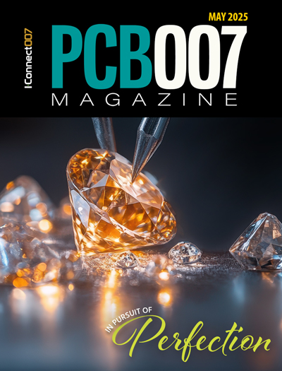
In Pursuit of Perfection: Defect Reduction
For bare PCB board fabrication, defect reduction is a critical aspect of a company's bottom line profitability. In this issue, we examine how imaging, etching, and plating processes can provide information and insight into reducing defects and increasing yields.

Voices of the Industry
We take the pulse of the PCB industry by sharing insights from leading fabricators and suppliers in this month's issue. We've gathered their thoughts on the new U.S. administration, spending, the war in Ukraine, and their most pressing needs. It’s an eye-opening and enlightening look behind the curtain.
- Articles
- Columns
- Links
- Media kit
||| MENU - pcb007 Magazine
Atotech Launches Pre Dip for Fine-Line Applications
March 21, 2018 | AtotechEstimated reading time: 1 minute
Neoganth W Pre Dip is Atotech’s new process for the desmear and metallization (PTH) process step for fine line HDI and package substrate applications. The new pre dip assures higher yield rates due to a significantly reduced occurrence of short circuits.
The trend for ever smaller lines and spaces in advanced HDI boards for mobile applications continues. Lines and spaces (L/S) will be reduced to 25/25 µm by 2019. The trend was made possible by manufacturing technologies such as modified semi-additive processes (mSAP) and advanced modified semi-additive processes (amSAP). With this minimization comes the need for new PORs (process of record), which offer significant technical advantages over existing ones.
Neoganth W Pre Dip
Atotech’s newly developed Neoganth W Pre Dip is a low foaming activator pre dip designed for horizontal transportation mode such as in Atotech’s Uniplate LB line. The process leads to a significant reduction in particle formation thereby enabling higher yield rates in fine line production. A key feature to achieve this is its alkaline pH.
Customer data has shown that using Neoganth W Pre Dip reduces the occurrence of short circuits in the process by up to 50% compared to competitive products. At the same time, the process provides excellent coverage performance while significantly reducing foaming behavior.
Coverage performance comparison on 4 different base materials (Isola IS410,Panasonic R1755C, Nanya NP140,Shengyi S1141) after new make-up, throughput and with maximum drag-in of Neoganth® W Pre Dip into the subsequent activator bath
Neoganth W Pre Dip is best used in front of an ionic PTH activator, such as Neoganth U Activator or Neoganth X Activator. It ensures proper wetting, pre-conditions the glass fibers and securely removes remaining copper oxides after etch cleaning.
The process has already been rolled-out successfully in Korea, Taiwan and China. Its key benefits allow it to exceed previous PTH POR process steps thereby assuring customers receive outstanding performance results.
About Atotech
Atotech is one of the world’s leading manufacturers of specialty chemicals and equipment for the printed circuit board, IC-substrate and semiconductor industries, as well as for the decorative and functional surface finishing industries. Atotech has annual sales of USD1.1 billion. The company is fully committed to sustainability – we develop technologies to minimize waste and to reduce environmental impact. Atotech has its headquarters in Berlin, Germany, and employs more than 4,000 people in over 40 countries. For more information, click here.
Suggested Items
The Evolution of Picosecond Laser Drilling
06/19/2025 | Marcy LaRont, PCB007 MagazineIs it hard to imagine a single laser pulse reduced not only from nanoseconds to picoseconds in its pulse duration, but even to femtoseconds? Well, buckle up because it seems we are there. In this interview, Dr. Stefan Rung, technical director of laser machines at Schmoll Maschinen GmbH, traces the technology trajectory of the laser drill from the CO2 laser to cutting-edge picosecond and hybrid laser drilling systems, highlighting the benefits and limitations of each method, and demonstrating how laser innovations are shaping the future of PCB fabrication.
Day 2: More Cutting-edge Insights at the EIPC Summer Conference
06/18/2025 | Pete Starkey, I-Connect007The European Institute for the PCB Community (EIPC) summer conference took place this year in Edinburgh, Scotland, June 3-4. This is the third of three articles on the conference. The other two cover Day 1’s sessions and the opening keynote speech. Below is a recap of the second day’s sessions.
Day 1: Cutting Edge Insights at the EIPC Summer Conference
06/17/2025 | Pete Starkey, I-Connect007The European Institute for the PCB Community (EIPC) Summer Conference took place this year in Edinburgh, Scotland, June 3-4. This is the second of three articles on the conference. The other two cover the keynote speeches and Day 2 of the technical conference. Below is a recap of the first day’s sessions.
Preventing Surface Prep Defects and Ensuring Reliability
06/10/2025 | Marcy LaRont, PCB007 MagazineIn printed circuit board (PCB) fabrication, surface preparation is a critical process that ensures strong adhesion, reliable plating, and long-term product performance. Without proper surface treatment, manufacturers may encounter defects such as delamination, poor solder mask adhesion, and plating failures. This article examines key surface preparation techniques, common defects resulting from improper processes, and real-world case studies that illustrate best practices.
RF PCB Design Tips and Tricks
05/08/2025 | Cherie Litson, EPTAC MIT CID/CID+There are many great books, videos, and information online about designing PCBs for RF circuits. A few of my favorite RF sources are Hans Rosenberg, Stephen Chavez, and Rick Hartley, but there are many more. These PCB design engineers have a very good perspective on what it takes to take an RF design from schematic concept to PCB layout.


