


 The Government Circuit: New Council Now Helps Shape Policy Decisions in the Electronics Supply Chain
 Learning With Leo: Soldering—The Interpretation Problem
 Nolan’s Notes: The ROI of Setup Optimization


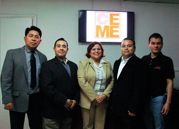
PAC Global Inc. and Competitive Edge Manufacturing Equipment (CEME) have joined the Saki America team in the Southern United States and Mexico. The companies are representing Saki's complete line of 2D and 3D automated solder paste, automated optical, and automated x-ray (SPI, AOI, and AXI) inspection and measurement systems and software and Saki's Smart manufacturing, Industry 4.0, and machine-2-machine initiatives.
PAC Global, with headquarters in Dallas, Texas, covers Texas, Oklahoma, Arkansas, Louisiana, and Mexico (except Sonora and the Baja area). PAC Global provides sales and applications support for the entire territory and is working with Saki to provide field service support for its customers in Mexico. PAC Global has a full staff of sales people, field service engineers, applications engineers, and administrative personnel. Besides its Dallas and Austin, TX offices, and its Mexico headquarters in Guadalajara, PAC Global has personnel located in Chihuahua, Juarez, Reynosa, Monterrey, and Queretaro, with training and demonstration centers in Guadalajara and Queretaro.
"Saki is a great addition to our portfolio," said Eric Culbertson, President of PAC Global. "We are a representative for FUJI Smart Factory with NEXIM, and Saki's inspection and measurement systems play an integral role in supporting that initiative."
CEME, based in Baja, California, handles sales and local direct applications and support for Saki in Baja. Founded in 1997, CEME provides world-class automated surface mount assembly equipment and software solutions and represents FUJI and other major companies.
"In today's rapidly changing environment we constantly strive to offer the most up-to-date products and solutions available," said Habacuc Molina, regional sales manager for CEME. "Saki will help our customers manufacture defect-free products at maximum throughput and efficiency."
"We are excited that PAC Global and CEME are representing Saki," said Satoshi Otake, general manager, Saki America. "Both companies have strong engineering backgrounds and are actively engaged in Business 4.0, Smart Factory, and M2M communication initiatives. They are known for their superior customer service and support. We look forward to collaborating with PAC Global and CEME to bring the fastest and most accurate inspection and measurement equipment to electronics manufacturing companies in the South Western US and Mexico."
About Saki
Since its inception in 1994, Saki has led the way in the development of automated recognition through robotic vision technology. Saki's 3D automated solder paste, optical, and x-ray inspection systems (SPI, AOI, AXI) have been recognized to provide the stable platform and advanced data capture mechanisms necessary for true M2M communication, improving production, process efficiency, and product quality. Saki Corporation has headquarters in Tokyo, Japan, with offices, sales, and support centers around the world. For more information click here.


