


 It’s Only Common Sense: Selling to Today's Generation of Buyers
 Dan’s Biz Bookshelf: ‘Believe in Better'
 The Big Picture: Our Big ‘Why’ in the Age of AI


Atotech to Demo Spherolyte CU UF3 for Fine Line RDL at ECTC 2018
May 17, 2018 | AtotechEstimated reading time: 2 minutes
Atotech will be exhibiting at the Electronics Components and Technology Conference (ECTC) 2018. As a gold sponsor, Atotech will participate with two presentations and a booth, highlighting its latest solutions for flexible electronics as well as fan-out wafer-level and fan-out panel-level packaging. The 68th ECTC will be held from May 29 to June 1, 2018, at the Sheraton San Diego Hotel and Marina in San Diego, California. Atotech’s international experts and specialists can be found at booth 207.
On Wednesday, May 30, from 8:00 – 8:25 am, Tobias Bernhard, Scientist for desmear and metallization at Atotech Deutschland GmbH, will talk about the “In-situ stress determination of electroless copper on PCB-relevant substrates”. The presentation is part of Session I on “Flexible Electronics, Substrates for High Frequency Applications” and takes place in Room Harbor Island 1. In his presentation, Tobias Bernhard will present the stress evolution of electroless Cu during and after deposition on ABF, Polyimide and on Ni-Fe in combination with Ni-containing and Ni-free commercial available electroless Cu baths.
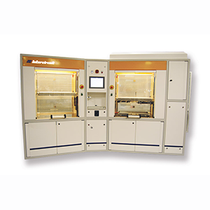
On Friday, June 1, from 10:50 – 11:15 am, Ralf Schmidt, Team Manager R&D for semiconductor technology at Atotech Deutschland GmbH, will present the “Optimization of electrodeposited copper for sub 5 µm L/S RDL lines by plating additives”. As part of Session 26 on “Wafer-Level Packaging Fan-In and Fan-Out Key Developments,” the presentation will be held in Room Harbor Island 2. In his presentation, Ralf Schmidt will present Atotech’s Spherolyte Cu UF3 process, which fulfills the requirements of current fine line RDL. This high-purity ECD Cu process is a three additive system designed for plating sub 5 µm Cu lines and large Cu pads while simultaneously enabling via filling.
Spherolyte Cu UF3: Micro via filling post anneal
The ECTC is one of the premier international events bringing together the best in packaging, components and microelectronic systems science, technology and education in an environment of cooperation and technical exchange. As such, it is the perfect place for companies like Atotech to present and exhibit their innovative systems and product solutions. The 2018 ECTC will feature, among others, about 40 technical sessions, 16 professional development courses, and a technology corner for exhibitors.
Visitors to the show are invited to join Atotech’s presentations or pass by booth 207 during the ECTC show. At the show, visitors can find out more about Atotech’s market-leading manufacturing tools, such as MultiPlate® - a systems solution for double sided (DS) ECD on wafer and DS electrolytic plating on glass panels. Atotech will also present its applications for the HDI, package substrate, semiconductor, flex/rigid-flex, PCB and IC leadframes markets. Local and international specialists will be on site to discuss any question or inquiry.
About Atotech
Atotech is one of the world’s leading manufacturers of specialty chemicals and equipment for the printed circuit board, IC-substrate and semiconductor industries, as well as for the decorative and functional surface finishing industries. Atotech has annual sales of USD1.2 billion (2017). The company is fully committed to sustainability – we develop technologies to minimize waste and to reduce environmental impact. Atotech has its headquarters in Berlin, Germany, and employs about 4,000 people in over 40 countries. About a quarter of all staff works in one of the four locations in Germany: Berlin, Feucht, Neuruppin, and Trebur. For more information, click here.
Share on:


Suggested Items
The Evolution of Picosecond Laser Drilling
06/19/2025 | Marcy LaRont, PCB007 MagazineIs it hard to imagine a single laser pulse reduced not only from nanoseconds to picoseconds in its pulse duration, but even to femtoseconds? Well, buckle up because it seems we are there. In this interview, Dr. Stefan Rung, technical director of laser machines at Schmoll Maschinen GmbH, traces the technology trajectory of the laser drill from the CO2 laser to cutting-edge picosecond and hybrid laser drilling systems, highlighting the benefits and limitations of each method, and demonstrating how laser innovations are shaping the future of PCB fabrication.
Day 2: More Cutting-edge Insights at the EIPC Summer Conference
06/18/2025 | Pete Starkey, I-Connect007The European Institute for the PCB Community (EIPC) summer conference took place this year in Edinburgh, Scotland, June 3-4. This is the third of three articles on the conference. The other two cover Day 1’s sessions and the opening keynote speech. Below is a recap of the second day’s sessions.
Day 1: Cutting Edge Insights at the EIPC Summer Conference
06/17/2025 | Pete Starkey, I-Connect007The European Institute for the PCB Community (EIPC) Summer Conference took place this year in Edinburgh, Scotland, June 3-4. This is the second of three articles on the conference. The other two cover the keynote speeches and Day 2 of the technical conference. Below is a recap of the first day’s sessions.
Preventing Surface Prep Defects and Ensuring Reliability
06/10/2025 | Marcy LaRont, PCB007 MagazineIn printed circuit board (PCB) fabrication, surface preparation is a critical process that ensures strong adhesion, reliable plating, and long-term product performance. Without proper surface treatment, manufacturers may encounter defects such as delamination, poor solder mask adhesion, and plating failures. This article examines key surface preparation techniques, common defects resulting from improper processes, and real-world case studies that illustrate best practices.
RF PCB Design Tips and Tricks
05/08/2025 | Cherie Litson, EPTAC MIT CID/CID+There are many great books, videos, and information online about designing PCBs for RF circuits. A few of my favorite RF sources are Hans Rosenberg, Stephen Chavez, and Rick Hartley, but there are many more. These PCB design engineers have a very good perspective on what it takes to take an RF design from schematic concept to PCB layout.