















 Dan’s Biz Bookshelf: ‘Building a Story Brand 2.0’
 It’s Only Common Sense: Why Should They Take Your Call?





It is becoming harder to respond to the demands of the rapidly-growing information society due to failures caused by increased chip temperatures in the ever-more integrated chips used by the latest electronic devices based on semiconductor materials. Therefore, the development of spin wave integrated circuits (ICs), which can perform information processing with minimal generation of heat by manipulating spin only rather than moving electrons, has been gaining attention.
Within this field, spin waves transmitted through a magnetic insulator film have the advantage that energy loss is small and long-distance transmission is possible. On the other hand, in order to transmit spin waves within a magnetic insulator film, it was previously necessary to attach relatively large permanent magnet parts to the magnetic insulator film, which was a problem for realizing spin wave ICs.
Taichi Goto at the Toyohashi University of Technology and Caroline Ross of the Massachusetts Institute of Technology and others collaborated to create a single-crystalline yttrium iron garnet (YIG) film, that is well-known as a magnetic insulator, on multiple substrates, and transmit the spin waves. Then, the influence of the magnitude of the stress in the magnetic insulator film on a spin wave was studied (Advanced Electronic Materials, "Static and Dynamic Magnetic Properties of Single-Crystalline Yttrium Iron Garnet Films Epitaxially Grown on Three Garnet Substrates").
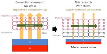
As a result, it was revealed that if the stress magnitude is large, spin waves are transmitted even if the attached permanent magnets are small (or weak). This is because if there is stress in the magnetic insulator film, it has the same effect as placing weak permanent magnets in close proximity.
The Relationship between Stress and Spin Wave
By clarifying the relationship between stress and spin wave in a magnetic insulator film, the size of the permanent magnets required for spin wave generation was able to be reduced. (Image: Toyohashi University of Technology)
According to Assistant Professor Goto, "YIG is one of the most noteworthy materials of late, and new devices and new phenomena using this technology, including spin waves, are being discovered one after another. Among these discoveries, we are leading the world in developing spin wave ICs using YIG. In the past, the relationship between the static magnetic response created by stress and the dynamic response that indicates the behavior of spin waves in YIG film was not well understood. This important development piece was what we wanted to put in place with this research."
Takuya Yoshimoto, a Research Fellow of the Japan Society for the Promotion of Science (JSPS), who worked on forming the samples, commented, "This research has yielded an equation that represents the relationship between stress and spin waves in magnetic insulator films. This is not only a very important step towards the realization of spin wave ICs but also accelerates the R&D on high frequency magnetic properties in the GHz band including spin waves and magnetic materials in the nano and micro scales."
In this research, a YIG thin film with a thickness of about 100 nm was formed on three garnet substrates with the same garnet structure as YIG but different lattice constants using pulsed laser deposition, and was used to investigate crystal structure, crystal strain, and stress magnitude.
A pair of electrodes for exciting and detecting spin waves was formed on the fabricated YIG using electron beam lithography, and the relationship between the external magnetic field and the propagation frequency of the spin wave was measured. The dispersion equation of the spin wave including the change in magnetic anisotropy due to crystal strain was calculated, and it was confirmed that the calculated results were almost equal to the measured results.
Also, by changing the magnitude of the generated strain, the size of the magnet required to excite the spin wave was able to be reduced by about 2.5 times compared to the case without strain. As a result, the whole spin wave IC can be miniaturized, and the device can be fabricated on a chip.
In the future, the research team will apply the spin wave multi-input/output phase interference device of this technique to real spin wave devices, with the initial aim of demonstrating the function of a spin wave IC fabricated on a chip.


