


 Driving Innovation: Direct Imaging vs. Conventional Exposure
 It’s Only Common Sense: Selling to Today's Generation of Buyers
 Dan’s Biz Bookshelf: ‘Believe in Better'


Tiny Defects in Semiconductors Created 'Speed Bumps' for Electrons
June 11, 2018 | UCLAEstimated reading time: 3 minutes
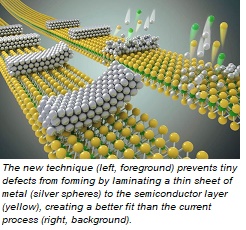
UCLA scientists and engineers have developed a new process for assembling semiconductor devices. The advance could lead to much more energy-efficient transistors for electronics and computer chips, diodes for solar cells and light-emitting diodes, and other semiconductor-based devices.
Their method joins a semiconductor layer and a metal electrode layer without the atomic-level defects that typically occur when other processes are used to build semiconductor-based devices. Even though those defects are minuscule, they can trap electrons traveling between the semiconductor and the adjacent metal electrodes, which makes the devices less efficient than they could be. The electrodes in semiconductor-based devices are what enable electrons to travel to and from the semiconductor; the electrons can carry computing information or energy to power a device.
Generally, metal electrodes in semiconductor devices are built using a process called physical vapor deposition. In this process, metallic materials are vaporized into atoms or atomic clusters that then condense onto the semiconductor, which can be silicon or another similar material. The metal atoms stick to the semiconductor through strong chemical bonds, eventually forming a thin film of electrodes atop the semiconductor.
One issue with that process is that the metal atoms are usually different sizes or shapes from the atoms in the semiconductor materials that they’re bonding to. As a result, the layers cannot form perfect one-to-one atomic connections, which is why small gaps or defects occur.
“It is like trying to fit one layer of Lego brand blocks onto those of a competitor brand,” Huang said. “You can force the two different blocks together, but the fit will not be perfect. With semiconductors, those imperfect chemical bonds lead to gaps where the two layers join, and those gaps could extend as defects beyond the interface and into the materials.”
Those defects trap electrons traveling across them, and the electrons need extra energy to get through those spots.
The UCLA method prevents the defects from forming, by joining a thin sheet of metal atop the semiconductor layer through a simple lamination process. And instead of using chemical bonds to hold the two components together, the new procedure uses van der Waals forces — weak electrostatic connections that are activated when atoms are very close to each other — to keep the molecules “attached” to each other. Van der Waals forces are weaker than chemical bonds, but they’re strong enough to hold the materials together because of how thin they are — each layer is around 10 nanometers thick or less.
“Even though they are different in their geometry, the two layers join without defects and stay in place due to the van der Waals forces,” Huang said.
The research is also the first work to validate a scientific theory that originated in the 1930s. The Schottky-Mott rule proposed the minimum amount of energy electrons need to travel between metal and a semiconductor under ideal conditions.
Using the theory, engineers should be able to select the metal that allows electrons to move across the junction between metal and semiconductor with the smallest amount of energy. But because of those tiny defects that have always occurred during manufacturing, semiconductor devices have always needed electrons with more energy than the theoretical minimum.
The UCLA team is the first to verify the theory in experiments with different combinations of metals and semiconductors. Because the electrons didn’t have to overcome the usual defects, they were able to travel with the minimum amount of energy predicted by the Schottky-Mott rule.
“Our study for the first time validates these fundamental limits of metal–semiconductor interfaces,” Duan said. “It shows a new way to integrate metals onto other surfaces without introducing defects. Broadly, this can be applied to the fabrication of any delicate material with interfaces that were previously plagued by defects.”
For example, besides electrode contacts on semiconductors, it could be used to assemble ultra–energy-efficient nanoscale electronic components, or optoelectronic devices such as solar cells.
The paper’s other UCLA authors are graduate students Jian Guo, Enbo Zhu and Sung-Joon Lee, and postdoctoral scholar Mengning Ding. Researchers from Hunan University, China; King Saud University, Saudia Arabia; and Northrop Grumman Corporation also contributed to the study.
The study builds off of nearly a decade of work by Duan and Huang on using van der Waals forces to integrate materials. A study they led, published in Nature in March 2018, described their use of van der Waals forces to create a new class of 2D materials called monolayer atomic crystal molecular superlattices. In an earlier study, which was published in Nature in 2010, they described their use of van der Waals forces to build high-speed transistors using graphene.
Share on:


Suggested Items
TRI to Unveil New High-Throughput AOI and AXI at productronica 2023
09/15/2023 | TRITest Research, Inc. (TRI), the leading test and inspection systems provider for the electronics manufacturing industry, will join productronica 2023, which will be held at Messe München Center from November 14 – 17, 2023.
UK Space Agency Launches Consultation on Variable Liability Limits for Orbital Operations
09/15/2023 | UK Space AgencyThe proposals from the UK Space Agency follow a review into the UK’s approach to setting the amount of an operator’s liability in licences for orbital operations, a key commitment of the government’s National Space Strategy.
MediaTek Successfully Develops First Chip Using TSMC's 3nm Process, Set for Volume Production in 2024
09/14/2023 | MediaTekMediaTek and TSMC announced that MediaTek has successfully developed its first chip using TSMC's leading-edge 3nm technology, taping out MediaTek’s flagship Dimensity system-on-chip (SoC) with volume production expected next year.
MKS’ Atotech to Participate in IPCA Expo 2023
09/14/2023 | MKS’ AtotechMKS’ Atotech, a leading surface finishing brand of MKS Instruments, will participate in the upcoming IPCA Expo at Bangalore International Exhibition Centre (BIEC) and showcase its latest PCB manufacturing solutions from September 13 – 15.
Comtech Unveils New BRIDGE Solutions to Increase Access to Global Hybrid Connectivity
09/12/2023 | Business WireComtech launched its new blended, resilient, integrated, digital, global, end-to-end (BRIDGE) connectivity solutions. Comtech’s BRIDGE solutions provide portable, adaptable, full-service communications networks that can be established in a matter of hours and help “bridge the gap” for traditional satellite and terrestrial infrastructures.