


 Learning with Leo: Drones—Meeting Demand Without Compromise
 Nolan’s Notes: Our Spotlight on North America
 Global Sourcing Spotlight: Building a Supply Chain That Bends, Not Breaks


Novel Approach to Void Reduction Using Microflux Coated Solder Preforms
July 26, 2018 | By A. Lifton, P. Salerno, J. Sidone and O. Khaselev, Alpha Assembly SolutionsEstimated reading time: 6 minutes
Bottom terminated component packages, such as QFN, are becoming increasingly relevant due to their ability to carry high-power dies in a small form factor. With increasing reliability performance requirements, power management components in packages like QFNs are critical to optimizing thermal and electrical performance. Additionally, low voiding is important for decreasing the current path of the circuit to maximize high-speed and RF performances. The market demand for void reduction under thermal pads of QFN components due to shrinking package sizes and increasing power requirements has generated the need to evaluate key process factors that contribute to voiding to design an optimal solution.
The addition of a micro-fluxed preform in conjunction with a low-voiding solder paste and process know-how is seen to create ideal solder volume with minimal voiding. As IPC 7093 specification acknowledges, one of the key concerns with bottom termination components (BTC) such as QFNs is achieving the solder volume required for a high-reliability solder joint. A multitude of processing factors such as reflow profile, reflow atmosphere, pad finish, and stencil design have been assessed in this study to develop a solution for achieving a high-reliability solder joint with low voiding for QFN packages.
Experimental Procedure
A full factorial DOE was designed based on key factors contributing to voiding under bottom termination components. The use of a solder preform was investigated compared to a solder paste only benchmark sample. The key factors in this DOE were identified and selected by subject matter experts from a leader in semiconductor manufacturing, an OEM of specialized test and measurement equipment for radio communications, and a solder manufacturer.
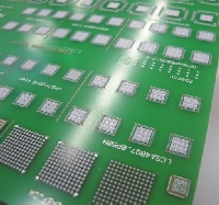
Figure 1: Image of the PCB test vehicle and some of the components used in this DOE.
A custom single layer 1.6 mm PCB test vehicle was designed specifically for this investigation that encompassed numerous variables that can contribute to voiding in bottom termination components. A single-layer PCB design (Figure 1) was chosen so that other factors (i.e., multilayer board and ground planes) would not influence the key factors being addressed in this study. QFN components of various sizes and pin configurations were among the variables addressed and further defined. In this study, only QFN components were selected (Table 1).
Table 1: Component details.
There were two types of test boards generated: one with an immersion tin (ImmSn) plating, which is widely used in automotive application and another with an immersion silver (ImmAg) plating, which is used in high-reliability and high-power application.
The test board also addressed via design including through hole via, no via, and plugged via configurations under the QFN and LCS components. The through hole via had a 0.3 mm diameter with and 0.5 mm diameter resist on top and bottom. The plugged via maintained the same 0.3 mm diameter hole and depth of 0.4 mm with 0.7 mm diameter resist on top and bottom. Vias were configured in a pattern as indicated in Figure 2.
Figure 2: Via design and configuration on the test vehicle.
The investigation also addressed reflow profile and reflow atmosphere. A low voiding SAC305, type 4 solder paste was used for this study with solidus temperature of 217°C and liquidus temperature 220°C. Thermocouples were strategically placed on the QFN32, and QFN64 component locations on the test vehicle. Proven straight ramp and high soak reflow profiles were evaluated as shown in Figure 3.
Figure 3: Reflow profiles using in this study.
The straight ramp profile increased at a rate of 1°C/s until reaching liquidus temperature of 220°C. The test vehicle was subjected to 65 seconds above liquidus (TAL) with peak temperature on the test vehicle reaching 240°C. The high-soak reflow profile increased temperature at a rate of 1°C/s up to 150°C before slowing to a rate of 0.5°C/s up to 200°C to allow more time for the flux to activate the surfaces.
Table 2: Assemblies' configuration details.
The high-soak profile subjected the test vehicle to 50 seconds above liquidus (220°C) with a peak temperature of 240°C on the test vehicle. Finally, both air and nitrogen reflow atmospheres were evaluated in this investigation to further understand the effect of voiding under bottom termination components.
The focus of the investigation involved the use of the micro-flux coated solder preform to increase solder volume relative to fluxing agent and reduce voiding. The use of a SAC305 microflux coated solder preform in conjunction with paste was benchmarked against a solder paste only test vehicle for each of the configurations summarized in Table 2. Four replicate boards of each iteration were processed to ensure statistically viable data.
Figure 4: Solder paste print configuration. (Examples of window pane solder prints on QFN components used in benchmark samples.)
Close to 2,000 data points were generated combining 54 components on each test vehicle and four replicates of each configuration. The solder paste only benchmark samples were printed in a window pane configuration commonly used in the industry for void reduction and shown in Figure 4.
The design of a solder preforms to allow intimate contact with the thermal pad of the component and increase solder volume played a significant role in the results presented in this investigation. Figure 5 represents an example of the use of solder paste only in window pane format on a QFN where mechanical stack-up issues on the component and reflow characteristics of solder paste make it difficult to achieve good voiding.
Page 1 of 2
Share on:


Testimonial
"We’re proud to call I-Connect007 a trusted partner. Their innovative approach and industry insight made our podcast collaboration a success by connecting us with the right audience and delivering real results."
Julia McCaffrey - NCAB GroupSuggested Items
I-Connect007 Editor’s Choice: Five Must-Reads for the Week
05/08/2026 | Marcy LaRont, I-Connect007This week, I’ve selected some outstanding interviews that you’ll want to take note of. First, is a roundtable discussion featuring three dynamic industry cybersecurity experts. Please watch this important discussion that affects us all. Following that, I spotlight the IPC-2581 Consortium, which explains why IPC-2581 is the standard to replace Gerber data for manufacturing. Next, I am including my interview with PCBAA and AAM, who collaborated to release a short documentary on U.S. PCB manufacturing.
Global Electronics Association to Testify at the Office of the U.S. Trade Representative Panel on Section 301 Structural Excess Capacity
05/08/2026 | Global Electronics AssociationChris Mitchell, Vice President for Global Government Relations at the Global Electronics Association, will testify before the Office of the U.S. Trade Representative (USTR) Panel on Section 301 Structural Excess Capacity on Friday, May 8.
Hall of Fame Spotlight Series: Highlighting Karen McConnell
05/07/2026 | Dan Feinberg, I-Connect007In 2021, Karen McConnell was awarded the Raymond E. Pritchard Hall of Fame award in recognition of her contributions to the Association and the electronics industry. As a senior staff member and CAD/CAM engineer at Northrop Grumman Enterprise Services, her primary responsibility was to develop a common, shared EDM (Electronic Document Management) library to support the electrical and PCB design tool initiatives across Northrop Grumman Mission Systems.
A Necessary Shift From Gerber to IPC-2581
05/07/2026 | Tracy Riggan, Global Electronics AssociationIPC-2581 is an open, vendor-neutral data exchange standard developed by the Global Electronics Association to streamline the exchange of PCB design information across fabrication, assembly, and test. It replaces multiple legacy formats—including industry standards, Gerber, and ODB++—with a single, comprehensive, XML-based dataset that captures all manufacturing details.
TTC-LLC and TTCI: Smarter Training, Stronger Test at PCB East 2026
04/27/2026 | The Test Connection Inc.The Training Connection LLC (TTC-LLC) and The Test Connection, Inc. (TTCI) will be exhibiting together at PCB East 2026, taking place April 28–May 1 at the DCU Convention Center in Worcester, Massachusetts. Attendees can find both teams at Booth #103 during the main exhibition day on Wednesday, April 29.