


 The Chemical Connection: Onshoring PCB Production—Daunting but Certainly Possible
 It’s Only Common Sense: The Phone Is Still Mightier Than the Keyboard


Large Supercrystals Promise Superior Sensors
August 2, 2018 | Sandia National LaboratoriesEstimated reading time: 2 minutes
Using an artful combination of nanotechnology and basic chemistry, Sandia National Laboratories researchers have encouraged gold nanoparticles to self-assemble into unusually large supercrystals that could significantly improve the detection sensitivity for chemicals in explosives or drugs.
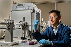
Image Caption: Sandia National Laboratories researcher Hongyou Fan holds a container enclosing gold supercrystals in front of a small-angle X-ray scattering instrument, one of the tools he uses to characterize his unusual creations. (Photo by Randy Montoya) Click on the thumbnail for a high-resolution image.
“Our supercrystals have more sensing capability than regular spectroscopy instruments currently in use, just like a dog’s nose has more sensing capabilities than a human’s,” said lead Sandia researcher Hongyou Fan.
Other researchers previously reported forming gold supercrystals but only in the micron range, too small for commercial production, said Fan, whose submillimeter supercrystals are easily manipulated with industrial tools of the macroworld.
The benchtop sensors, recently reported in Nature Communications, also are surprisingly inexpensive, Fan says. “The supercrystals are built of gold, but only a little of it.” It takes 0.012 grams of gold to form a sensor, for a total materials cost of roughly 50 cents.
To form each of the Sandia supercrystals, millions of gold nanoparticles tightly self-assemble in orderly rows. The particles naturally develop facets — resembling those cut in diamonds by a jeweler — to exist at the lowest possible energy level needed to maintain the existence of the crystal.
Crystal facets ‘bay’ like hounds
The facets are adept at recognizing and transmitting signals. They “bay” in groups like hounds — that is, emit a strong signal — when a predetermined external frequency is “sniffed.” That is because when a nanoparticle recognizes a band frequency and makes it resonate, that energy will pass to other nanoparticles, coupled by nearness and the local electromagnetic field. The alerted nanoparticles augment the response in a kind of echoing action, making noticeable what in less keen sensors may have passed unnoticed.
The initial formation of the crystals involves dispersing gold particulates about 5 nanometers in diameter into a “good” solvent, toluene. They then are subjected to a bath in a “hostile” solvent, isopropanol, which the particles supersaturate and from which they are then ejected or precipitated.
The ejected particles, refugees from the solution, then crystallize as small seeds. The growth of facets makes them available to respond to a wide variety of incoming chemical odors or light band frequencies.
The proper concentrations of materials and particle immersion times are important factors in creating large crystals. The process may take as long as a week.
Share on:


Testimonial
"We’re proud to call I-Connect007 a trusted partner. Their innovative approach and industry insight made our podcast collaboration a success by connecting us with the right audience and delivering real results."
Julia McCaffrey - NCAB GroupSuggested Items
How PCBA Excellence Transforms High-mix Operations
09/22/2025 | Chintan Sanghani, Electronics Center for ExcellenceWith over 30 years of manufacturing excellence, our organization has built deep expertise in PCBA contract manufacturing for downhole oilfield tools. Through years of focused operational leadership in this demanding sector, we've learned that in high-mix, low-volume (HMLV) environments, traditional manufacturing approaches can create more bottlenecks than breakthroughs.
Advint Incorporated Brings Artificial Intelligence to Electroplating Training
09/11/2025 | Advint IncorporatedAdvint Incorporated is introducing a new dimension to its electroplating training programs: the integration of Artificial Intelligence (AI). This initiative reflects the company’s commitment to providing PCB fabricators and manufacturers in the USA and Canada with training that is practical, forward-looking, and directly relevant to today’s production challenges.
The Signal Integrity Issue: Design007 Magazine September 2025
09/09/2025 | I-Connect007 Editorial TeamAs the saying goes, “If you don’t have signal integrity problems now, you will eventually.” This month, our experts share a variety of design techniques that can help PCB designers and design engineers achieve signal integrity.
Semiconductors Get Magnetic Boost with New Method from UCLA Researchers
07/31/2025 | UCLA NewsroomA new method for combining magnetic elements with semiconductors — which are vital materials for computers and other electronic devices — was unveiled by a research team led by the California NanoSystems Institute at UCLA.
SMT Perspectives and Prospects: Warren Buffett’s Perpetual Wisdom, Part 1
07/29/2025 | Dr. Jennie Hwang -- Column: SMT Perspectives and ProspectsOver the years, I have cherished the lessons by Warren Buffett and Charlie Munger at the Berkshire Hathaway annual shareholders meeting in Omaha, Nebraska. This year, I was among the more than 40,000 who attended the May 3 meeting. Millions more from around the world, including from the UK, Germany, Japan, China, Panama, and Guatemala, tuned in remotely and via CNBC’s livestream.