


 The Marketing Minute: Marketing With Layers
 The Right Approach: Electro-Tek—A Williams Family Legacy, Part 1
 It’s Only Common Sense: If You’re Not Differentiated, You’re Dead


Inkjet Printers Can Produce Cheap Micro-Waveguides for Optical Computers
November 26, 2018 | ITMO UniversityEstimated reading time: 2 minutes
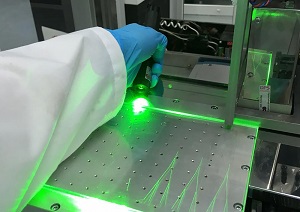
Scientists from ITMO University have proposed a new technology for creating optical micro-waveguides based on inkjet printing. By using this method, it is possible to create waveguides with the necessary parameters quickly and without expensive equipment and complex procedures. The new technology is now being optimized for the production of optical elements on an industrial scale.
Today, optical fiber is widely used in communication. Many people know that it can transmit a signal over long distances with minimal losses, providing us, as an example, with stable and high-speed Internet. However, as devices become smaller and smaller, scientists and engineers have come up with an analog of fiber on a microscale. Such devices are called waveguides. They are integral in creating new-generation computers on an optical basis, serving to ensure efficient signal transmission and processing.
Most researchers now suggest complex and expensive technologies for creating waveguides, such as laser ablation or photolithography. These are time-consuming procedures requiring complex equipment, rare materials and additional sample processing. But scientists from ITMO University have developed an alternative method for creating optical micro-waveguides. It is based on a common inkjet technology.
Waveguide printing begins with the preparation of special ink. Its main ingredient is a suspended solution, or sol, of titanium dioxide nanoparticles. This material was chosen due to its high refractive index, which is necessary for the waveguide to effectively conduct the signal. In order to achieve suitable ink parameters, the scientists selected the right solvents, concentration of the main component, and surfactants. After that the ink is filled into an inkjet printer, which applies the material according to a given geometry on a clean glass substrate.
“The defining feature of our work is that we explained the choice of material, as well as the working wavelength and waveguide geometry, instead of just simply describing the properties and methods. Its main advantage, however, is that it offers a simple and cheap technique suitable for industry. This work was aimed at a practically applicable result since the very beginning, and now we have conducted the first industrial tests of our technology together with the IQDemy company. The results confirmed that the method can be upscaled without losing the waveguides quality,” comments Anastasiia Klestova, member of the SCAMT Laboratory of ITMO University.
It isn’t only the industrial adaptation of the waveguide inkjet printing technique that the scientists are currently focusing on. Their plans for the near future include applying inkjet printing in the production of other elements necessary for processing optical signal.
“It is obvious that the creation of elements of data storage and transmission based on the photons movement control is the fundamental technology for future computers. The most difficult part in the engineering of such devices is the development of efficient signal transport lines. But our solution removes all the major limitations in this area, and I have no doubt that soon we will see photon computing devices with waveguides created with our method,” notes Alexander Vinogradov, researcher at the SCAMT Laboratory of ITMO University.
Share on:


Testimonial
"Advertising in PCB007 Magazine has been a great way to showcase our bare board testers to the right audience. The I-Connect007 team makes the process smooth and professional. We’re proud to be featured in such a trusted publication."
Klaus Koziol - atgSuggested Items
TRI to Unveil New High-Throughput AOI and AXI at productronica 2023
09/15/2023 | TRITest Research, Inc. (TRI), the leading test and inspection systems provider for the electronics manufacturing industry, will join productronica 2023, which will be held at Messe München Center from November 14 – 17, 2023.
UK Space Agency Launches Consultation on Variable Liability Limits for Orbital Operations
09/15/2023 | UK Space AgencyThe proposals from the UK Space Agency follow a review into the UK’s approach to setting the amount of an operator’s liability in licences for orbital operations, a key commitment of the government’s National Space Strategy.
MediaTek Successfully Develops First Chip Using TSMC's 3nm Process, Set for Volume Production in 2024
09/14/2023 | MediaTekMediaTek and TSMC announced that MediaTek has successfully developed its first chip using TSMC's leading-edge 3nm technology, taping out MediaTek’s flagship Dimensity system-on-chip (SoC) with volume production expected next year.
MKS’ Atotech to Participate in IPCA Expo 2023
09/14/2023 | MKS’ AtotechMKS’ Atotech, a leading surface finishing brand of MKS Instruments, will participate in the upcoming IPCA Expo at Bangalore International Exhibition Centre (BIEC) and showcase its latest PCB manufacturing solutions from September 13 – 15.
Comtech Unveils New BRIDGE Solutions to Increase Access to Global Hybrid Connectivity
09/12/2023 | Business WireComtech launched its new blended, resilient, integrated, digital, global, end-to-end (BRIDGE) connectivity solutions. Comtech’s BRIDGE solutions provide portable, adaptable, full-service communications networks that can be established in a matter of hours and help “bridge the gap” for traditional satellite and terrestrial infrastructures.