


 Dan’s Biz Bookshelf: ‘Dream First, Details Later
 Happy’s Tech Talk #40: Factors in PTH Reliability—Hole Voids
 Facing the Future: Time for Real Talk, Early and Often, Between Design and Fabrication


Atotech Brings World-Class AHDI to the U.S.
December 6, 2018 | I-Connect007 Editorial TeamEstimated reading time: 1 minute
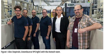
During our walk-through of the GreenSource Fabrication facility with VP Alex Stepinski, he started the conversation on surface preparation and plating by saying, “We have Atotech horizontal production technology in place here. We’ve been running Atotech turnkey solutions for a while. All of the equipment and chemistry are from Germany. They come here and configure everything for us. Our three biggest suppliers are Atotech, Schmoll, and AWP. With Atotech, we have direct support from Germany on a regular basis here. We’re doing real technology development with Atotech.”
The Atotech equipment is central to the operation of GreenSource Fabrication. Over the course of the week, we took a deeper dive into Atotech’s installations there. We had several conversations with four Atotech representatives on site to oversee the installation: Moody Dreiza, business director for electronics in North America; Daniel Schmidt, global director for marketing electronics and corporate technology training; Kuldip Johal, global original equipment manufacturer (OEM) director for new technology/pathfinding; and John Foley, systems engineer for the GreenSource facility.
Our conversations explored the specifics for each Atotech line in the GreenSource facility. We discussed production equipment, chemistry, capabilities, and unique innovations specifically developed to realize Stepinski’s vision of highest production flexibility.
Barry Matties: Could you give us an overview of the Atotech equipment installed here at GreenSource?
Daniel Schmidt: Today, GreenSource has eight Atotech production lines installed, including three copper platers, two electroless cop per lines, two surface treatment lines, and a direct metallization line. GreenSource also uses a variety of different Atotech wet chemistry processes, such as our high-throw electroless copper (Printoganth T1), blind microvia filling process (Inpulse 2HF), electrolyte for through-hole, BMV and conformal plating (Inpulse 2THF), electrolyte for conformal or flash plating (Inpulse 2HT), as well as laser direct drilling pretreatment (BondFilm LDD SR), higher copper loading bonding enhancement (BondFilm HC), and our ENIG process (Aurotech DC).
To read the full version of this article which originally appeared in the October 2018 SMT007 Magazine, click here.
Share on:


Suggested Items
I-Connect007 Editor’s Choice: Five Must-Reads for the Week
07/11/2025 | Andy Shaughnessy, Design007 MagazineThis week, we have quite a variety of news items and articles for you. News continues to stream out of Washington, D.C., with tariffs rearing their controversial head again. Because these tariffs are targeted at overseas copper manufacturers, this news has a direct effect on our industry.I-Connect007 Editor’s Choice: Five Must-Reads for the Week
Digital Twin Concept in Copper Electroplating Process Performance
07/11/2025 | Aga Franczak, Robrecht Belis, Elsyca N.V.PCB manufacturing involves transforming a design into a physical board while meeting specific requirements. Understanding these design specifications is crucial, as they directly impact the PCB's fabrication process, performance, and yield rate. One key design specification is copper thieving—the addition of “dummy” pads across the surface that are plated along with the features designed on the outer layers. The purpose of the process is to provide a uniform distribution of copper across the outer layers to make the plating current density and plating in the holes more uniform.
Trump Copper Tariffs Spark Concern
07/10/2025 | I-Connect007 Editorial TeamPresident Donald Trump stated on July 8 that he plans to impose a 50% tariff on copper imports, sparking concern in a global industry whose output is critical to electric vehicles, military hardware, semiconductors, and a wide range of consumer goods. According to Yahoo Finance, copper futures climbed over 2% following tariff confirmation.
Happy’s Tech Talk #40: Factors in PTH Reliability—Hole Voids
07/09/2025 | Happy Holden -- Column: Happy’s Tech TalkWhen we consider via reliability, the major contributing factors are typically processing deviations. These can be subtle and not always visible. One particularly insightful column was by Mike Carano, “Causes of Plating Voids, Pre-electroless Copper,” where he outlined some of the possible causes of hole defects for both plated through-hole (PTH) and blind vias.
Trouble in Your Tank: Can You Drill the Perfect Hole?
07/07/2025 | Michael Carano -- Column: Trouble in Your TankIn the movie “Friday Night Lights,” the head football coach (played by Billy Bob Thornton) addresses his high school football team on a hot day in August in West Texas. He asks his players one question: “Can you be perfect?” That is an interesting question, in football and the printed circuit board fabrication world, where being perfect is somewhat elusive. When it comes to mechanical drilling and via formation, can you drill the perfect hole time after time?