


 American Made Advocacy: Rebuilding America’s Military Stockpiles Begins With Microelectronics
 The Right Approach: The End of an Era—DoD Proposes MIL-PRF-31032 Cancellation
 Defense Speak Interpreted: Hypersonics Report Back After Six Years of Silence


SMT Electrolytic Capacitor Solder Joint Criteria and Integrity Investigation
December 21, 2018 | David Hillman, Rockwell CollinsEstimated reading time: 7 minutes
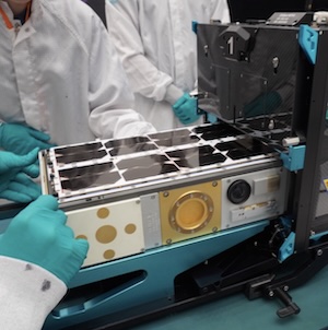
Figure 5: Assembly showing SMT electrolytic capacitor locations.
Figure 6: Typical SMT electrolytic capacitors. (Photo courtesy of Conrad Dubilier)
Assembly
The test vehicles were assembled at the Rockwell Collins Coralville, IA production facility. The solder paste was Henkel MP-218 tin lead eutectic solder deposited with a 0.005 inch thick stencil. The components were placed using a Universal Advantis automated placement machine. The assemblies were reflowed in a Heller 1912EXL Reflow Oven. Assemblies were cleaned in the Electrovert Aquastorm 200 inline cleaner. The majority of the solder joint is obscured due to the package configuration, with only the outer end of the component lead being visible for optical inspection (Figure 8). The portions of the solder joints that were visually inspectable were considered non-compliant as they did not meet a 1T minimum side fillet height. The typical placement/spacing of the SMT electrolytic capacitors makes solder joint touch-up challenging and creates a potential opportunity for component or laminate damage.
Thermal Cycle Testing
The test vehicles were placed into a thermal chamber set for a temperature range of -55°C to 125°C. The ramp rate was set for 5°C–10°C per minute with 10-minute dwells at each temperature extreme. Figure 9 shows the thermal profile.
Figure 7: Typical SMT electrolytic capacitors. (Photo Courtesy of Panasonic).
After completing a total of 532 thermal cycles, the components were removed from the thermal cycle chamber for metallographic cross-sectional analysis.
Shear Testing
Prior to thermal cycle testing, a set of electrolytic capacitors were carefully removed from the assembled test vehicles for shear testing. This data set documented the typical as-soldered, not thermal cycled condition to provide a measurement of the strength of the solder joint wetting/geometry configuration. An Instron test system using a shear rate of 0.15 inches/minute was used for the test.
Figure 10 illustrates the test components/shear test setup. The measured mean peak load for the shear testing was 40.3 pounds with a standard deviation of 5.4 pounds (Figure 11). There are no industry acknowledged minimum shear force values, however, 30 pounds would be considered very adequate for solder joint integrity.
For comparison, the typical component pad peel strength is 6-12 pounds.
Figure 8: Optical view of solder joints after automated reflow soldering.
Optical examination of the failed solder joints after shear testing revealed minor solder joint voiding, good wetting/solder joint geometry and complete metallurgical attachment for both the solder joint/component lead interface and the solder joint/component pad interface (i.e. cohesive failure).
Figure 12 illustrate the typical failed solder joint interfaces resulting from the shear testing.
Metallographic Analysis
A number of the SMT electrolytic capacitors were removed from the test vehicle after the completion of the thermal cycle conditioning for metallographic analysis. Some very minor cracking was observed in the solder joint heel fillet region but there were no observed anomalies in the solder joint microstructure or cracking that would indicate degradation of the solder joint integrity due to thermal cycle conditioning (Figure 13).
It was noted that a “1T” solder joint heel fillet or side fillet was not achieved using the standard automated reflow soldering process. The solder joint heel fillet height was found to be in the 1/2T height range.
Figure 14 through Figure 16 illustrate the solder fillet heights achieved with the standard automated reflow soldering process.
Figure 14: Cross sectional toe view of SMT electrolytic capacitor illustrating ~ 63% T side fillet height.
Figure 15: Cross sectional toe view of SMT electrolytic capacitor illustrating ~ 54% T side fillet height.
Page 2 of 3
Share on:


Testimonial
"Your magazines are a great platform for people to exchange knowledge. Thank you for the work that you do."
Simon Khesin - Schmoll MaschinenSuggested Items
Indium to Showcase High-Performance AI Application Solutions at SEMICON SEA 2026
05/01/2026 | Indium CorporationAs a leading provider of advanced materials solutions for today’s demanding AI applications, Indium Corporation® will feature its high-reliability product portfolio at SEMICON SEA 2026, May 5-7, in Kuala Lumpur, Malaysia.
ACCM Unveils Negative and Near-zero CTE Materials for Large-Format AI Chips
04/21/2026 | Advanced Chip and Circuit MaterialsAdvanced Chip and Circuit Materials, Inc. (ACCM) has launched two new materials: Celeritas HM50, with a negative coefficient of thermal expansion (CTE) of -8 ppm/°C to offset the positive CTE and expansion of copper with temperature on circuit boards, and Celeritas HM001, with near-zero CTE and the low-loss performance needed for high-speed signal layers to 224 Gb/s and faster in artificial intelligence (AI) circuits.
SMTA Ultra HDI Symposium, Day 2: Fragile Supply Chains, Fierce Innovation
04/14/2026 | Marcy LaRont, I-Connect007The Arizona weather yielded another beautiful day as we gathered for the second day of SMTA’s annual UHDI symposium. After the first full day discussing the role of AI in business and the how-tos of implementation, Avondale Mayor Mike Pineda kicked off day two, proud to showcase his city and to declare its important place in the continued development of the West Valley, an increasingly important area for tech and manufacturing.
KYZEN Focuses on Aqueous and Stencil Cleaning Solutions at SMTA Monterrey Expo and Tech Forum
04/10/2026 | KYZEN'KYZEN, the global leader in innovative environmentally friendly cleaning chemistries, will exhibit at the SMTA Monterrey Expo & Tech Forum.
Solder Paste Innovations for Enhanced Reliability from MacDermid Alpha Electronics Solutions
04/10/2026 | Real Time with... APEX EXPOJason Fullerton of MacDermid Alpha Electronics Solutions discusses innovative alloys like Innolot MXE, low-temperature solder options, and polymer reinforcement strategies. Learn how these solutions address the growing demands of high-performance computing and larger component assemblies, ensuring optimal performance and cost-effectiveness.