


 Beyond Design: The Fundamental Structure of Spectral Integrity
 Elementary, Mr. Watson: High Power: When Physics Becomes Real
 The Shaughnessy Report: Watt About Power Integrity?


A Microscope as a Shovel? UConn Researchers Dig It
January 29, 2019 | University of ConnecticutEstimated reading time: 4 minutes
Using a familiar tool in a way it was never intended to be used opens up a whole new method to explore materials, report UConn researchers in Proceedings of the National Academies of Science. Their specific findings could someday create much more energy-efficient computer chips, but the new technique itself could open up new discoveries in a broad range of stuffs.
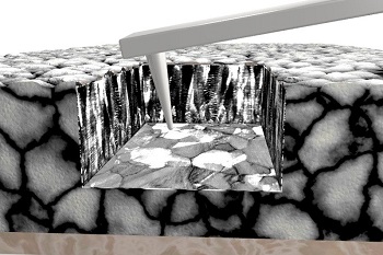
Image Caption: Bryan Huey’s lab used the tip of an Atomic Force Microscope (AFM) as a chisel to scrape away the surface of bismuth ferrite and map the electric landscape of the interior. (Image courtesy of the Huey Lab)
Atomic force microscopes (AFM) drag an ultra sharp tip across materials, ever so close but never touching the surface. The tip can feel where the surface is, detecting electric and magnetic forces produced by the material. By methodically passing it back and forth, a researcher can map out the surface properties of a material in the same way a surveyor methodically paces across a piece of land to map the territory. AFMs can give a map of a material’s holes, protrusions, and properties at a scale thousands of times smaller than a grain of salt.
Image Caption: A new domain. The researchers were able to show how the domains (tiny sections of material with the same electric polarization) in the bismuth ferrite changed in shape with depth. (Image courtesy of the Huey Lab)
AFMs are designed to investigate surfaces. Most of the time, the user tries very hard not to actually bump the material with the tip, as that could damage the surface of the material. But sometimes it happens. A few years ago, graduate student Yasemin Kutes and Justin Luria, a postdoc, studying solar cells in materials science and engineering professor Bryan Huey’s lab, accidentally dug into their sample. At first thinking it was an irritating mistake, they did notice that the properties of the material looked different when Kutes stuck the tip of the AFM deep into the ditch she’d accidentally dug.
Kutes and Luria didn’t pursue it. But another graduate student, James Steffes, was inspired to look more closely at the idea. What would happen if you intentionally used the tip of an AFM like a chisel, and dug into a material, he wondered? Would it be able to map out the electrical and magnetic properties layer by layer, building up a 3D picture of the material’s properties the same way it mapped the surface in 2D? And would the properties look any different deep inside a material?
The answers, Steffes, Huey, and their colleagues report in PNAS, are yes and yes. They dug into a sample of bismuth ferrite (BiFeO3), which is a room temperature multiferroic. Multiferroics are materials that can have multiple electric or magnetic properties at the same time. For example, bismuth ferrite is both antiferromagnetic – it responds to magnetic fields, but overall doesn’t exhibit a North or South magnetic pole – and ferroelectric, meaning it has switchable electric polarization. Such ferroelectric materials are usually composed of tiny sections, called domains. Each domain is like a cluster of batteries that all have their positive terminals aligned in the same direction. The clusters on either side of that domain will be pointed in another direction. They are very valuable for computer memory, because the computer can flip the domains, ‘writing’ on the material, using magnetic or electric fields.
When a materials scientist reads or writes information on a piece of bismuth ferrite, they can normally only see what happens on the surface. But they would love to know what happens below the surface — if that was understood, it might be possible to engineer the material into more efficient computer chips that run faster and use less energy than the ones available today. That could make a big difference in society’s overall energy consumption – already, 5 percent of all electricity consumed in the US goes to running computers.
To find out, Steffes, Huey, and the rest of the team used an AFM tip to meticulously dig through a film of bismuth ferrite and map out the interior, piece by piece. They found they could map the individual domains all the way down, exposing patterns and properties that weren’t always apparent at the surface. Sometimes a domain narrowed until it vanished or split into a y-shape, or merged with another domain. No one had ever been able to see inside the material in this way before. It was revelatory, like looking at a 3D CT scan of a bone when you’d only been able to read 2D X-rays before.
“Worldwide, there are something like 30,000 AFMs already installed. A big fraction of those are going to try [3D mapping with] AFM in 2019, as our community realizes they have just been scratching the surface this whole time,” Huey predicts. He also thinks more labs will buy AFMs now if 3D mapping is demonstrated to work for their materials, and some microscope manufacturers will start designing AFMs specifically for 3D scanning.
Steffes has subsequently graduated from UConn with his Ph.D. and now works at GlobalFoundries, a computer chip maker. Researchers at Intel, muRata, and elsewhere are also intrigued with what the group found out about bismuth ferrite, as they seek new materials to make the next generation of computer chips. Huey’s team, meanwhile, is now using AFMs to dig into all kinds of materials, from concrete to bone to a host of computer components.
“Working with academic and corporate partners, we can use our new insight to understand how to better engineer these materials to use less energy, optimize their performance, and improve their reliability and lifetime – those are examples of what materials scientists strive to do every day,” Huey says.
Share on:


Testimonial
"Our marketing partnership with I-Connect007 is already delivering. Just a day after our press release went live, we received a direct inquiry about our updated products!"
Rachael Temple - AlltematedSuggested Items
ITW EAE Despatch Ovens Now Support ASTM 5423 Testing
10/15/2025 | ITW EAEAs the demand for high-performance electrical insulation materials continues to grow—driven by the rapid expansion of electric vehicles (EVs) and energy storage systems—thermal processing has become a critical step in material development.
Beyond Thermal Conductivity: Exploring Polymer-based TIM Strategies for High-power-density Electronics
10/13/2025 | Padmanabha Shakthivelu and Nico Bruijnis, MacDermid Alpha Electronics SolutionsAs power density and thermal loads continue to increase, effective thermal management becomes increasingly important. Rapid and efficient heat transfer from power semiconductor chip packages is essential for achieving optimal performance and ensuring long-term reliability of temperature-sensitive components. This is particularly crucial in power systems that support advanced applications such as green energy generation, electric vehicles, aerospace, and defense, along with high-speed computing for data centers and artificial intelligence (AI).
Is Glass Finally Coming of Age?
10/13/2025 | Nolan Johnson, I-Connect007Substrates, by definition, form the base of all electronic devices. Whether discussing silicon wafers for semiconductors, glass-and-epoxy materials in printed circuits, or the base of choice for interposers, all these materials function as substrates. While other substrates have come and gone, silicon and FR-4 have remained the de facto standards for the industry.
Creative Materials to Showcase Innovative Functional Inks for Medical Devices at COMPAMED 2025
10/09/2025 | Creative Materials, Inc.Creative Materials, a leading manufacturer of high-performance functional inks and coatings, is pleased to announce its participation in COMPAMED 2025, taking place November 17–20 in Düsseldorf, Germany.
Jiva Leading the Charge Toward Sustainable Innovation
09/30/2025 | Marcy LaRont, PCB007 MagazineEnvironmental sustainability in business—product circularity—is a high priority these days. “Circularity,” the term meant to replace “recycling,” in its simplest definition, describes a full circle life for electronic products and all their elements. The result is re-use or a near-complete reintroduction of the base materials back into the supply chain, leaving very little left for waste. For what cannot be reused productively, the ultimate hope is to have better, less harmful means of disposal and/or materials that can seamlessly and harmlessly decompose and integrate back into the natural environment. That is where Jiva and Soluboard come in.