


 The Marketing Minute: Marketing With Layers
 The Right Approach: Electro-Tek—A Williams Family Legacy, Part 1
 It’s Only Common Sense: If You’re Not Differentiated, You’re Dead


Breakthrough in Graphene Research
January 31, 2019 | FAUEstimated reading time: 3 minutes
Graphene is a promising material for use in nanoelectronics. Its electronic properties depend greatly, however, on how the edges of the carbon layer are formed. Zigzag patterns are particularly interesting in this respect, but until now it has been virtually impossible to create edges with a pattern like this.
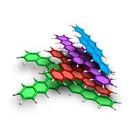
Image Caption: The much sought-after zigzag pattern can be found either in staggered rows of honeycombs (blue and purple) or four-limbed stars surrounding a central point of four graphene honeycombs (red and green). (Image: FAU/Konstantin Amsharov)
Chemists and physicists at FAU have now succeeded in producing stable nanographene with a zigzag edge. Not only that, the method they used was even comparatively simple. Their research, conducted within the framework of collaborative research centre 953—Synthetic Carbon Allotropes funded by the German Research Foundation (DFG), has now been published in the journal Nature Communications*.
Image Caption: Different patterns are formed at the edges of nanographene. Zigzags are particularly interesting – and particularly unstable. FAU researchers have now succeeded in creating stable layers of carbon with this pattern on their edges. (Image: FAU/Konstantin Amsharov)
Bay, fjord, cove, armchair and zigzag—when chemists use terms such as these, it is clear that they are referring to nanographene. More specifically, the shape taken by the edges of nanographene, i.e. small fragments of graphene. Graphene consists of a single-layered carbon structure, where each carbon atom is surrounded by three others. This creates a pattern reminiscent of a honeycomb, with atoms in each of the corners. Nanographene is a promising candidate for use in the field of microelectronics, taking over from silicon which is used today and bringing microelectronics down to the nano scale.
The electronic properties of the material depend greatly on its shape, size and above all, periphery, in other words how the edges are structured. A zigzag periphery is particularly suitable, as in this case the electrons, which act as charge carriers, are more mobile than in other edge structures. This means that using pieces of zigzag-shaped graphene in nanoelectronic components may allow higher frequencies for switches.
The problem currently faced by materials scientists who want to research only zigzag nanographene is that this form makes the compounds rather unstable, and unable to be produced in a controlled manner. This is a prerequisite, however, if the electronic properties are to be investigated in detail.
The team of researchers led by PD Dr. Konstantin Amsharov from the Chair of Organic Chemistry II have now succeeded in doing just that. Not only have they discovered a straightforward method for synthesising zigzag nanographene, their procedure delivers a yield of close to one hundred percent and is suitable for large scale production. They have already produced a technically relevant quantity in the laboratory.
First of all, the FAU researchers produce preliminary molecules, which they then fitt together in a honeycomb formation over several cycles, in a process known as cyclisation. In the end, graphene fragments are produced from staggered rows of honeycombs or four-limbed stars surrounding a central point of four graphene honeycombs, with the sought-after zigzag pattern to their edges. Why is this method able to produce stable zigzag nanographene? The explanation lies in the fact that the product crystallises directly even during synthesis. In their solid state, the molecules are not in contact with oxygen. In solution, however, oxidation causes the structures to disintegrate quickly.
This approach allows scientists to produce large pieces of graphene, whilst maintaining control over their shape and periphery. This breakthrough in graphene research means that scientists should soon be able to produce and research a variety of interesting nanographene structures, a crucial step towards finally being able to use the material in nanoelectronic components.
Share on:


Testimonial
"In a year when every marketing dollar mattered, I chose to keep I-Connect007 in our 2025 plan. Their commitment to high-quality, insightful content aligns with Koh Young’s values and helps readers navigate a changing industry. "
Brent Fischthal - Koh YoungSuggested Items
HPE Now Powers New AI-Ready Supercomputer Set to Transform Environmental Forecasting in New Zealand
09/22/2025 | BUSINESS WIREHPE announced that Earth Sciences New Zealand (formally NIWA) of Aotearoa (New Zealand) selected HPE Cray XD2000, purpose-built for AI and simulation workloads, to accelerate the organization’s environmental science and precision of meteorological forecasting.
PC Graphics Add-in Board Shipments Up 27% QoQ in 2Q25
09/03/2025 | Jon Peddie ResearchAccording to a new research report from the analyst firm Jon Peddie Research, the growth of the global PC-based graphics add-in board market reached 11.6 million units in Q2'25 and desktop PC CPUs shipments increased to 21.7 million units.
PC GPU Shipments Up 8.4% in 2Q25 on Pre-Tariff Demand
09/02/2025 | Jon Peddie ResearchJon Peddie Research reports the growth of the global PC-based graphics processor unit (GPU) market reached 74.7 million units in Q2'25, and PC CPU shipments increased to 66.9 million units.
20 Years of Center Nanoelectronic Technologies (CNT) – Backbone of German Semiconductor Research Celebrates Anniversary
08/14/2025 | Fraunhofer IPMSThe Center Nanoelectronic Technologies (CNT) of the Fraunhofer Institute for Photonic Microsystems (IPMS) is celebrating its 20th anniversary this year. Since its founding in 2005, it has developed into a pillar of applied semiconductor research in Germany and Europe. With its unique research cleanroom and equipment adhering to the 300-mm wafer industry standard, CNT is unparalleled in Germany and serves as a central innovation driver for the microelectronics industry.
Q2 Client CPU Shipments Increased 8% from Last Quarter, Up 13% YoY
08/13/2025 | Jon Peddie ResearchJon Peddie Research reports that the global client CPU market expanded for two quarters in a row, and in Q2’25, it showed unseasonal growth of 7.9% from last quarter, while server CPU shipments increased 22% year over year.