-

- News
- Books
Featured Books
- smt007 Magazine
Latest Issues
Current Issue
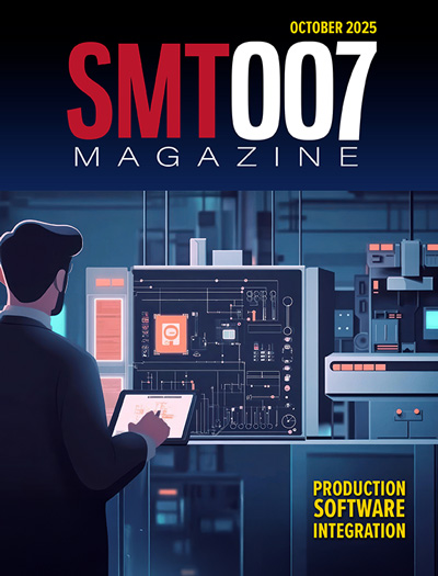
Production Software Integration
EMS companies need advanced software systems to thrive and compete. But these systems require significant effort to integrate and deploy. What is the reality, and how can we make it easier for everyone?

Spotlight on India
We invite you on a virtual tour of India’s thriving ecosystem, guided by the Global Electronics Association’s India office staff, who share their insights into the region’s growth and opportunities.

Supply Chain Strategies
A successful brand is built on strong customer relationships—anchored by a well-orchestrated supply chain at its core. This month, we look at how managing your supply chain directly influences customer perception.
- Articles
- Columns
- Links
- Media kit
||| MENU - smt007 Magazine
KYZEN to Exhibit at Philippine Semiconductor & Electronics Convention and Exhibition
May 17, 2019 | KyzenEstimated reading time: 1 minute
KYZEN will exhibit at the 16th Philippine Semiconductor & Electronics Convention and Exhibition (PSECE), scheduled to take place May 30-June 1, 2019 at the SMX Convention Center in Pasay City, Manila. The company will showcase its AQUANOX A4727 Next Generation Aqueous Assembly Cleaner and MICRONOX MX2322 Solvent.
MICRONOX MX2322 is a semiconductor grade engineered semi aqueous solvent designed to clean all types of paste fluxes common in wafer bumping, wafer level packaging, die attach, flip chip and SiP that contain copper pillar. MX2322 has a wide process window, as well as a long bath life, to remove tough flux residue at a fast rate and is compatible with all sensitive metals. The solvent demonstrates its excellent cleaning performance and benefits in single-wafer spray-in-air tools as well as all immersion cleaning systems.
AQUANOX A4727 is engineered to be effective, stable and predictable, all day, every day. It is designed for reliable production and assembly operations. Meet your performance cleaning requirements with advanced technology that gives a stable pH and predictable compatibility throughout its long bath life.
AQUANOX A4727 is the result of thousands of hours of laboratory tests and “live” beta site testing scientifically validating the outstanding rinsability, extended bath life and consistently reliable, long-term performance advantages. This stable chemistry is proven to be compatible on a wide variety of components, coating, labels and equipment.
Environmentally responsible, AQUANOX A4727 is non-hazardous and biodegradable. It contains no CFCs or HAPs and can be used at low concentrations to effectively remove even the toughest soils, and rinse easily and completely. This easy to control and cost-effective solution is a good choice for both in-line and batch cleaning systems.
About KYZEN
KYZEN is a global leader in providing environmentally responsible, RoHS compliant precision cleaning chemistries for industries ranging from electronics and advanced packaging to metal finishing and aerospace applications. Since its founding in 1990, KYZEN’s innovative cleaning technologies, scientific expertise and customer support have been repeatedly recognized with the industry’s most prestigious awards. For more information, visit www.kyzen.com.
Testimonial
"Advertising in PCB007 Magazine has been a great way to showcase our bare board testers to the right audience. The I-Connect007 team makes the process smooth and professional. We’re proud to be featured in such a trusted publication."
Klaus Koziol - atgSuggested Items
Episode 6 of Ultra HDI Podcast Series Explores Copper-filled Microvias in Advanced PCB Design and Fabrication
10/15/2025 | I-Connect007I-Connect007 has released Episode 6 of its acclaimed On the Line with... American Standard Circuits: Ultra High Density Interconnect (UHDI) podcast series. In this episode, “Copper Filling of Vias,” host Nolan Johnson once again welcomes John Johnson, Director of Quality and Advanced Technology at American Standard Circuits, for a deep dive into the pros and cons of copper plating microvias—from both the fabricator’s and designer’s perspectives.
Nolan’s Notes: Tariffs, Technologies, and Optimization
10/01/2025 | Nolan Johnson -- Column: Nolan's NotesLast month, SMT007 Magazine spotlighted India, and boy, did we pick a good time to do so. Tariff and trade news involving India was breaking like a storm surge. The U.S. tariffs shifted India from one of the most favorable trade agreements to the least favorable. Electronics continue to be exempt for the time being, but lest you think that we’re free and clear because we manufacture electronics, steel and aluminum are specifically called out at the 50% tariff levels.
MacDermid Alpha & Graphic PLC Lead UK’s First Horizontal Electroless Copper Installation
09/30/2025 | MacDermid Alpha & Graphic PLCMacDermid Alpha Electronics Solutions, a leading supplier of integrated materials and chemistries to the electronics industry, is proud to support Graphic PLC, a Somacis company, with the installation of the first horizontal electroless copper metallization process in the UK.
Electrodeposited Copper Foils Market to Grow by $11.7 Billion Over 2025-2032
09/18/2025 | Globe NewswireThe global electrodeposited copper foils market is poised for dynamic growth, driven by the rising adoption in advanced electronics and renewable energy storage solutions.
MacDermid Alpha Showcases Advanced Interconnect Solutions at PCIM Asia 2025
09/18/2025 | MacDermid Alpha Electronics SolutionsMacDermid Alpha Electronic Solutions, a global leader in materials for power electronics and semiconductor assembly, will showcase its latest interconnect innovations in electronic interconnect materials at PCIM Asia 2025, held from September 24 to 26 at the Shanghai New International Expo Centre, Booth N5-E30


