


 Learning with Leo: Drones—Meeting Demand Without Compromise
 Nolan’s Notes: Our Spotlight on North America
 Global Sourcing Spotlight: Building a Supply Chain That Bends, Not Breaks


3D Optical Inspection Provides ‘Eyes’ for Process Improvements in Industry 4.0
June 21, 2019 | Jenny Yuh, Koh Young Technology, and Brent Fischthal, Koh Young AmericaEstimated reading time: 3 minutes
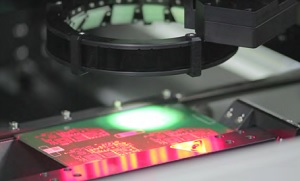
Automated 3D solder paste inspection (SPI) and 3D automated optical inspection (AOI) systems have become an integral part of the printed circuit board assembly (PCBA) process because they help ensure high-quality production. As today’s board complexity is increasing, inspection technology becomes even more critical.
For example, while talking with Janet Tomor, senior business development manager at Suntronic Inc.—a contract manufacturer with facilities in Richardson and Houston, Texas—I-Connect007 Managing Editor, Nolan Johnson asked, “Streamlining must be something you talk about a lot [at Suntronic].”
Tomor replied, “The biggest impact for us has been automating almost everything except for putting your through-hole connector on the board by hand. We’ve automated most of our inspection and have improved quality. We went from 60% yield on our PCBA lines to 98.9% by adding automated 3D inspection from Koh Young.”
Tomor’s team also added 3D SPI equipment, continuing, “I’ll give you an example. We have a solder paste inspection machine on every line. We once put on a stencil, and it wouldn’t pass. The cause was that the stencil was too thick and applied too much solder paste. We would have had parts sliding all over the board because of the excess solder paste. That was a huge discovery and a change we made thanks to our SPI.”
While most manufacturers base quality decisions on a “good-bad” comparison of reference images, these decisions are easily influenced by variables like surface finish, board condition, component proximity, and more. However, data generated from 3D measurement systems provides meaningful insights about the process and helps manufacturers identify and eliminate the root causes of a defect. When manufacturers trust the data from the system, this helps to transform their operations and accurately control and monitor the PCBA process. What are the requirements of an inspection system to move from inspection to measurement, and ultimately to process control and optimization? Simply stated, the systems must satisfy the three “Rs” for measurement data: reliable, repeatable, and relatable.
When Johnson asked Tomor which equipment they were using to automate inspection, her answer was straightforward: “Koh Young.”
Reliable
Koh Young’s implementation of full 3D coverage monitors performance to detect common defects, such as missing or wrong components, and accurately identifies other issues, such as coplanarity and lead bridging. By measuring components and solder joints, and then offering critical height information to the inspection algorithms, contract manufacturers can use reliable measurements to identify errors during the production process. For example, after Suntronic adopted Koh Young 3D inspection solutions, their yields increased into the high 90% range, which has helped to transform their operations. But what’s next?
How can they continue to improve? Tomor further commented, “We also have a post-reflow AOI after the oven tells us if anything shifted. It uses true 3D technology, so it can measure if the part is skewed, missing, shifted, tombstoned, etc. Between the Koh Young SPI and AOI solutions, we increased our yield.” When asked what else helps with streamlining the assembly process, Tomor simply stated, “New equipment helps a lot.”
That new equipment solution, though, pays off by prioritizing data over raw throughput. Global competition means that manufacturers place challenging demands on process solutions. Manufacturers want to monitor and adapt the process to achieve zero defects by accessing all of the data anytime, anywhere. Moreover, manufacturers want process optimization. 3D inspection solutions have been instrumental in providing better data in the form of body and lead tip measurement, allowing the new equipment to quantify shape, coplanarity, solder amount, etc.
To read the full article, which appeared in the June 2019 issue of SMT007 Magazine, click here.
Share on:


Testimonial
"In a year when every marketing dollar mattered, I chose to keep I-Connect007 in our 2025 plan. Their commitment to high-quality, insightful content aligns with Koh Young’s values and helps readers navigate a changing industry. "
Brent Fischthal - Koh YoungSuggested Items
AQUANOX A4727 and A4625 Lead KYZEN Offerings at SMTA Oregon Expo and Tech Forum
05/06/2026 | KYZENKYZEN, the global leader in innovative environmentally responsible cleaning chemistries, will exhibit at the SMTA Oregon Expo and Tech Forum scheduled to take place Thursday, May 19 at the Wingspan Event and Conference Center in Hillsboro, Oregon.
Connect the Dots: Designing for the Future of Manufacturing Reality—Surface Finish
05/07/2026 | Matt Stevenson -- Column: Connect the DotsWhen designing the complex boards that many electronic devices require to operate, designers should consider manufacturability at every step. This is my last article focused on designing for the always-evolving manufacturing reality. Choosing the right surface finish has always been important. If you are creating intricate designs with a wide variety of components, like for an ultra-high density interconnect (UHDI) board, surface finish is a critical last step.
Indium to Showcase High-Performance AI Application Solutions at SEMICON SEA 2026
05/01/2026 | Indium CorporationAs a leading provider of advanced materials solutions for today’s demanding AI applications, Indium Corporation® will feature its high-reliability product portfolio at SEMICON SEA 2026, May 5-7, in Kuala Lumpur, Malaysia.
ACCM Unveils Negative and Near-zero CTE Materials for Large-Format AI Chips
04/21/2026 | Advanced Chip and Circuit MaterialsAdvanced Chip and Circuit Materials, Inc. (ACCM) has launched two new materials: Celeritas HM50, with a negative coefficient of thermal expansion (CTE) of -8 ppm/°C to offset the positive CTE and expansion of copper with temperature on circuit boards, and Celeritas HM001, with near-zero CTE and the low-loss performance needed for high-speed signal layers to 224 Gb/s and faster in artificial intelligence (AI) circuits.
SMTA Ultra HDI Symposium, Day 2: Fragile Supply Chains, Fierce Innovation
04/14/2026 | Marcy LaRont, I-Connect007The Arizona weather yielded another beautiful day as we gathered for the second day of SMTA’s annual UHDI symposium. After the first full day discussing the role of AI in business and the how-tos of implementation, Avondale Mayor Mike Pineda kicked off day two, proud to showcase his city and to declare its important place in the continued development of the West Valley, an increasingly important area for tech and manufacturing.