


 Standard of Excellence: Speed vs. Quality in Customer Service
 Knocking Down the Bone Pile: Revamp Your Components with BGA Reballing
 Global Sourcing Spotlight: Balancing Speed and Flexibility Without Sacrificing Control


Practical Implementation of Assembly Processes for Low Melting Point Solder Pastes (Part 2)
July 24, 2019 | Adam Murling, Miloš Lazić, and Don Wood, Indium Corporation; and Martin Anselm, Rochester Institute of TechnologyEstimated reading time: 4 minutes
In the last three to five years, there has been a resurgence of interest in the use of low melting point alloys for SMT applications. Typically, the compositions are around the eutectic bismuth-tin alloy, perhaps with additions of other elements to increase the robustness of certain alloy properties. Now, there are several new products on the market and numerous ongoing reliability projects in industry consortia.
Alloy reliability is usually the main focus of the ongoing research, but this study will investigate the processability of these new materials and considerations to implement a new low melting point solder paste assembly process. Data previously presented in Part 1 of this article compared the stencil printing performance of some of these materials to leading next-generation, Pb-free, no-clean materials. This part will focus on a discussion of reflow approaches for the best success. Indium Corporation previously printed and tested four solder pastes: a bismuth-containing baseline (57Bi/42Sn/1Ag), two novel bismuth-based alloys, and an indium-based alloy.
Figure 1: Testing matrix.
All solder pastes used were brought to room temperature before stencil printing. Common, commercially available equipment was used for test board preparation. The test matrix in Figure 1 shows which reflow profiles were tested for each alloy. These solder pastes were exposed to two different reflow profiles on virgin copper-OSP metalized boards. The reflow profiles varied in time-above-liquidus (time and temperature), peak oven temperature, and conveyor speeds (25 inches per minute and 11.3 inches per minute). Detailed profiles are provided in Figures 3 and 4.
Reflow Results
There were two different reflow profiles used in an eight-zone reflow oven. The “slow” reflow process had a 205°C peak temperature, a conveyor speed of 11.3 inches/minute and a TAL (120°C) of 120 seconds (Figure 2). The “fast” reflow process had a 190°C peak temperature, but the conveyor speed was much faster (25 inches/minute) with a TAL (140°C) of 165 seconds (Figure 3).
Figure 2: Slow reflow profile with conveyor speed of 11.3 inches/minute.
Figure 3: Fast reflow profile with conveyor speed of 25 inches/minute.
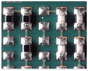
All three bismuth alloys were reflowed in both processes. The indium-based alloy was reflowed only with the slow reflow profile due to the peak temperature of the fast profile not being hot enough to promote adequate reflow. Examples of cross print and 0201 placement can be seen in Figures 4–10.
Figure 4: Baseline alloy with slow profile (L) and fast profile (R).
In Figure 4, the difference is apparent in the number of pads that wet together; the slow profile exhibits more instances where the solder deposits coalesce on the cross-print section of the test board. The fast profile is a standard recommended profile for the bismuth-tin eutectic alloy and exhibits shinier solder deposits than the slow profile.
Figure 5: Bismuth alloy 1 with slow profile (L) and fast profile (R).
Figure 6: Bismuth alloy 2 with slow profile (L) and fast profile (R).
Figures 5 and 6 show that the fast profile offers a better reflowed solder appearance and less bridging than using the slow profile.
Figure 7: Indium alloy with slow profile.
The indium alloy (Figure 7), when compared to the bismuth alloys, offers less bridging and shinier joints while comparing the slow profiles.
Figures 8 and 9 show that the fast profile offers a better reflowed solder appearance and less bridging than using the slow profile. The indium alloy (Figure 17), when compared to the bismuth alloys, offers less bridging and shinier joints while comparing the slow profiles.
The alloys in the placement portion of the test exhibited less difference and sensitivity to reflow profiles than the cross-printing portion. The preferred soldering profile for each alloy resulted in a more ideal solder joint appearance.
Figure 8: Baseline alloy 0201 placement slow profile (L) and fast profile (R).
Figure 9: Bismuth alloy 2 0201 placement slow profile (L) and fast profile (R).
Conclusion
Figure 10: Indium alloy 0201 placement slow profile.
In conclusion, the differences between the alloys vary when considering which test you are investigating. The print quality test offers the conclusion that the bismuth alloys have a better release, printability, and response-to-pause performance than the indium-containing one. Although the reflow portion offers the opposite, the indium-containing alloy offers a more desirable solder joint appearance, with the caveat that it was reflowed using only an optimized profile. This is because the alloy would not reflow at the lower temperatures of the fast profile, which was adequate and ideal for the bismuth-containing alloys.
Since the same flux was used for all of the solder pastes in this study, there is no comparison to legacy solder pastes. However, the printing performance on challenging area ratios clearly shows that the new materials are up to the standards expected for modern solder pastes. This will be critical to the development of low melting point solder pastes for the future.
Future Work
In the next phase of this research, BGAs and QFNs will be considered with regard to voiding performance. At this time, further reliability tests will allow the opportunity to attempt to characterize how each of the alloys behaves in regard to long-term reliability and failure modes.
Acknowledgments
David Sbiroli, technical manager, global accounts, Indium Corporation
Eric Bastow, assistant technical manager, America’s region, Indium Corporation
Meagan Sloan, technical support engineer, Indium Corporation
Rochester Institute of Technology
This paper was originally presented at the Technical Proceedings of SMTA International 2018.
Share on:


Testimonial
"Advertising in PCB007 Magazine has been a great way to showcase our bare board testers to the right audience. The I-Connect007 team makes the process smooth and professional. We’re proud to be featured in such a trusted publication."
Klaus Koziol - atgSuggested Items
BTU International Earns 2025 Step-by-Step Excellence Award for Its Aqua Scrub™ Flux Management System
10/29/2025 | BTU International, Inc.BTU International, Inc., a leading supplier of advanced thermal processing equipment for the electronics manufacturing market, has been recognized with a 2025 Step-by-Step Excellence Award (SbSEA) for its Aqua Scrub™ Flux Management Technology, featured on the company’s Pyramax™ and Aurora™ reflow ovens.
On the Line With… Ultra HDI Podcast—Episode 7: “Solder Mask: Beyond the Traces,” Now Available
10/31/2025 | I-Connect007I-Connect007 is excited to announce the release of the seventh episode of its 12-part podcast series, On the Line With… American Standard Circuits: Ultra HDI. In this episode, “Solder Mask: Beyond the Traces,” host Nolan Johnson sits down with John Johnson, Director of Quality and Advanced Technology at American Standard Circuits, to explore the essential role that solder mask plays in the Ultra HDI (UHDI) manufacturing process.
Rehm Wins Mexico Technology Award for CondensoXLine with Formic Acid
10/17/2025 | Rehm Thermal SystemsModern electronics manufacturing requires technologies with high reliability. By using formic acid in convection, condensation, and contact soldering, Rehm Thermal Systems’ equipment ensures reliable, void-free solder joints — even when using flux-free solder pastes.
Indium Experts to Deliver Technical Presentations at SMTA International
10/14/2025 | Indium CorporationAs one of the leading materials providers to the power electronics assembly industry, Indium Corporation experts will share their technical insight on a wide range of innovative solder solutions at SMTA International (SMTAI), to be held October 19-23 in Rosemont, Illinois.
Knocking Down the Bone Pile: Revamp Your Components with BGA Reballing
10/14/2025 | Nash Bell -- Column: Knocking Down the Bone PileBall grid array (BGA) components evolved from pin grid array (PGA) devices, carrying over many of the same electrical benefits while introducing a more compact and efficient interconnect format. Instead of discrete leads, BGAs rely on solder balls on the underside of the package to connect to the PCB. In some advanced designs, solder balls are on both the PCB and the BGA package. In stacked configurations, such as package-on-package (PoP), these solder balls also interconnect multiple packages, enabling higher functionality in a smaller footprint.