


 Dan’s Biz Bookshelf: ‘Dream First, Details Later
 Happy’s Tech Talk #40: Factors in PTH Reliability—Hole Voids
 Facing the Future: Time for Real Talk, Early and Often, Between Design and Fabrication


Interconnect Reliability Correlation With System Design and Transportation Stress
August 19, 2019 | Dr. Paul Wang, Vincent Weng, and Dr. Kim Sang Chim, Mitac International Inc.Estimated reading time: 4 minutes
Abstract
Interconnect reliability—especially in BGA solder joints and compliant pins, which are subjected to design parameters—is very critical to ensure product performance at predefined shipping conditions and user environments. Plating thickness of the compliant pin and the damping mechanism of electronic system design are key success factors for this purpose. In addition, transportation and material handling process of a computer server system will be affected by shock under certain conditions. Many accessory devices in the server computer system tend to become loose, resulting in poor contact or solder intermittent interconnect problems due to the shock load from the transportation and material handling processes.
Figure 1: Example of partial loose contact of a daughter card from a press-fit connector.
In this article, design variables—such as pin hard gold plating thickness, motherboard locking mechanism, and damping structure design—are experimented and reviewed. Also, a shock measurement device is used to real-time monitor the acceleration, duration, and direction of shock in large stationary or moving systems in transportation and transferring process. There were two transportation routes from Fushan, China, to Sezimovo, Czech Republic, through the China and Russia border by train and returned by sea cargo through the Mediterranean, Arabic, and South China Seas in which a product package was embedded with a shock measurement device. The collected force data of g-force can be used to calculate the shock energy level, ΔV. The comparison between the value of ΔV and shock energy tested in the lab can be used to judge whether a system design can sustain and cause contact interconnect problems in the transportation and transferring process. These design variables and stresses can be evaluated by drop test or vibration test to ensure system functional integrity is achieved.
Introduction
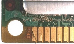
Figure 2: Dust and fiber accumulated in DIMM slot (L) and particles found near DIMM contact pads (R).
Reliability of BGA solder joints and compliant pin interconnects is critical to ensure product performance is maintained at predefined shipping conditions and user environments. Many electronic devices—such as network cards HDDs in the server system—tend to become loose, resulting in poor contact problems due to the severe shock from the transportation and material handling processes. Different design variables—such as hard gold plating thickness on the pin, motherboard locking mechanism, and damping plate—are experimented and reviewed in this article. A shock measuring device was used to monitor in real-time the acceleration, duration, and direction of shock in large stationary or moving systems in the transportation and transferring process.
Poor contact issues happened on some models of desktop, AIO, and server computer systems. After removing the top cover of a computer system, some accessories—such as memory and NIC cards—were found to be partially disengaged from their normal interconnect positions (Figure 1). An example of a contact interconnect defect rate for a specific experimental test vehicle is shown in Table 1. In most of the cases, these contact problems may not be permanent but can be quickly resolved by double insertion of the interconnect system.
Table 1: Defect rate of a series of computer server systems.
Although not the main topic of this study, another source of contact interconnect problems is coming from particles or fibers from raw material, manufacturing, or the user environment can be observed from time to time in DIMM socket pins and circuit board contact pads. These foreign materials can create a barrier for proper contact between pad and socket (Figure 2). In one extreme case, soft white plastic particles were smeared on the contact surface, creating a risk of intermittent contact or open circuit. FTIR organic chemical analysis indicated that the fibers were rayon/ cellulose, which is a common material from various sources—such as cloth and gloves—which are difficult to clearly implicate in a failure. However, the white particles are most likely polyethylene from plasticizer—a fatty acid that poses an interconnect concern (Table 2).
Table 2: Chemical analysis of foreign material on contact pads.
To avoid the accumulation of fibers and particles on contact pads, there are many changes required in environment control and management for sensitive interconnect devices, such as press-fit pins and optical modules. The use of particle counters is getting popular in particulate control on the manufacturing floor along with connector vacuuming, cleaning, and reseating/inserting an edge card. Again, in most cases, these contact problems may not be permanent but can be quickly resolved by double insertion of the interconnect system to provide a clean contact interconnect interface.
Approach
In this study, a realistic test vehicle is designed with a commercially available press-fit connector of various sources on to a motherboard with full electrical function. A riser card is plugged into the press-fit connector that serves as an interface for NIC and SSL card interconnect. The following three design variables were experimented on in addition to the pallet of test vehicles with an installed shock measurement device were shipped through two shipping routes as train and sea cargo to see the correlation to the function failure of the test vehicle:
• Damping plate for NIC and SSL cards
• Hard gold plating thickness
• Locking mechanism for motherboard
To read the full article, which appeared in the July 2019 issue of PCB007 Magazine, click here.
Share on:


Suggested Items
SHENMAO Strengthens Semiconductor Capabilities with Acquisition of PMTC
07/10/2025 | SHENMAOSHENMAO America, Inc. has announced the acquisition of Profound Material Technology Co., Ltd. (PMTC), a premier Taiwan-based manufacturer of high-performance solder balls for semiconductor packaging.
KYZEN to Highlight Understencil and PCB Cleaners at SMTA Querétaro Expo and Tech Forum
07/09/2025 | KYZEN'KYZEN, the global leader in innovative environmentally responsible cleaning chemistries, will exhibit at the SMTA Querétaro Expo & Tech Forum, scheduled to take place Thursday, July 24, at Centro de Congresos y Teatro Metropolitano de Querétaro.
Driving Innovation: Direct Imaging vs. Conventional Exposure
07/01/2025 | Simon Khesin -- Column: Driving InnovationMy first camera used Kodak film. I even experimented with developing photos in the bathroom, though I usually dropped the film off at a Kodak center and received the prints two weeks later, only to discover that some images were out of focus or poorly framed. Today, every smartphone contains a high-quality camera capable of producing stunning images instantly.
Hands-On Demos Now Available for Apollo Seiko’s EF and AF Selective Soldering Lines
06/30/2025 | Apollo SeikoApollo Seiko, a leading innovator in soldering technology, is excited to spotlight its expanded lineup of EF and AF Series Selective Soldering Systems, now available for live demonstrations in its newly dedicated demo room.
Indium Corporation Expert to Present on Automotive and Industrial Solder Bonding Solutions at Global Electronics Association Workshop
06/26/2025 | IndiumIndium Corporation Principal Engineer, Advanced Materials, Andy Mackie, Ph.D., MSc, will deliver a technical presentation on innovative solder bonding solutions for automotive and industrial applications at the Global Electronics A