


 Learning with Leo: Drones—Meeting Demand Without Compromise
 Nolan’s Notes: Our Spotlight on North America
 Global Sourcing Spotlight: Building a Supply Chain That Bends, Not Breaks


Development of Flexible Hybrid Electronics
August 14, 2019 | Weifeng Liu, PhD, FlexEstimated reading time: 2 minutes
Introduction
Flexible hybrid electronics (FHE) refers to a category of flexible electronics that are made through a combination of traditional assembly process of electronic components with high-precision ink printing technologies . By integrating silicon components with printed inks and flexible substrates, FHE will revolutionize the IoT and wearable industries. With FHE, designers can create a heterogeneous electronic system that can be fully integrated with different sensors, lighter in weight, more cost effective, more flexible and conforming to the curves of a human body or even stretchable across the shape of an object or structure—all while preserving the full functionality of traditional electronic systems.
The FHE industry is still in the early stages of development, and a variety of design, material, assembly and reliability issues need to be addressed. For example, electrical interconnections formed with conductive adhesives may not be as conductive or reliable as compared to conventional solder assembly. Typical polymer-based conductive inks are not as conductive as the etched copper used to make circuit boards and they are mostly not readily solderable. Additionally, commercially available stretchable thermoplastic-based film substrates have relatively low heat resistance and cannot withstand the current lead-free reflow process temperatures.
This article will present a hybrid manufacturing process to manufacture FHE systems with a two-layer interconnect structure utilizing screen printing of silver conductive ink, filled microvias to connect ink traces at the different layers, and use of the traditional reflow process to attach the semiconductor chips to the printed substrates.
Experimental
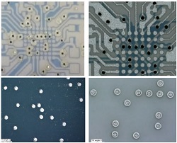
This study is to convert a rigid multilayer wearable development platform into a flexible one using printed conductive ink and flexible substrate. The current rigid platform contains two active semiconductor components and dozens of passive devices. The largest component is the microprocessor chip. Figure 1 shows the footprint for the microprocessor chip. It is an LGA package with 8X8 array and 64 I/Os. The pad size is 250 mm and the pitch is 400 mm, which leaves the space between pads at 150 mm.
To read this entire article, which appeared in the July 2019 issue of Design007 Magazine, click here.
Share on:


Testimonial
"The I-Connect007 team is outstanding—kind, responsive, and a true marketing partner. Their design team created fresh, eye-catching ads, and their editorial support polished our content to let our brand shine. Thank you all! "
Sweeney Ng - CEE PCBSuggested Items
AQUANOX A4727 and A4625 Lead KYZEN Offerings at SMTA Oregon Expo and Tech Forum
05/06/2026 | KYZENKYZEN, the global leader in innovative environmentally responsible cleaning chemistries, will exhibit at the SMTA Oregon Expo and Tech Forum scheduled to take place Thursday, May 19 at the Wingspan Event and Conference Center in Hillsboro, Oregon.
Connect the Dots: Designing for the Future of Manufacturing Reality—Surface Finish
05/07/2026 | Matt Stevenson -- Column: Connect the DotsWhen designing the complex boards that many electronic devices require to operate, designers should consider manufacturability at every step. This is my last article focused on designing for the always-evolving manufacturing reality. Choosing the right surface finish has always been important. If you are creating intricate designs with a wide variety of components, like for an ultra-high density interconnect (UHDI) board, surface finish is a critical last step.
Indium to Showcase High-Performance AI Application Solutions at SEMICON SEA 2026
05/01/2026 | Indium CorporationAs a leading provider of advanced materials solutions for today’s demanding AI applications, Indium Corporation® will feature its high-reliability product portfolio at SEMICON SEA 2026, May 5-7, in Kuala Lumpur, Malaysia.
ACCM Unveils Negative and Near-zero CTE Materials for Large-Format AI Chips
04/21/2026 | Advanced Chip and Circuit MaterialsAdvanced Chip and Circuit Materials, Inc. (ACCM) has launched two new materials: Celeritas HM50, with a negative coefficient of thermal expansion (CTE) of -8 ppm/°C to offset the positive CTE and expansion of copper with temperature on circuit boards, and Celeritas HM001, with near-zero CTE and the low-loss performance needed for high-speed signal layers to 224 Gb/s and faster in artificial intelligence (AI) circuits.
SMTA Ultra HDI Symposium, Day 2: Fragile Supply Chains, Fierce Innovation
04/14/2026 | Marcy LaRont, I-Connect007The Arizona weather yielded another beautiful day as we gathered for the second day of SMTA’s annual UHDI symposium. After the first full day discussing the role of AI in business and the how-tos of implementation, Avondale Mayor Mike Pineda kicked off day two, proud to showcase his city and to declare its important place in the continued development of the West Valley, an increasingly important area for tech and manufacturing.