


 Dan’s Biz Bookshelf: ‘Dream First, Details Later
 Happy’s Tech Talk #40: Factors in PTH Reliability—Hole Voids
 Facing the Future: Time for Real Talk, Early and Often, Between Design and Fabrication


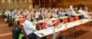
EIPC Summer Conference 2019, Day 2
September 12, 2019 | Alun Morgan, EIPCEstimated reading time: 11 minutes
Editor's note: Click here to read Part 1.
EIPC Board Member Christian Behrendt of Ilfa opened the second day as moderator of the session covering design process reliability. Behrendt was kind enough to thank EIPC Executive Director Kirsten Smit-Westenberg and EIPC Project Manager Carol Pelzers for their excellent organisation of the conference.
The first paper of the session was presented by Lars Böttcher of Fraunhofer IZM and was entitled “High-Density RDL Technologies for Fan-Out Panel Level Packaging.” His paper began with a description of the current practice of embedded packaging technologies with connections fanned out of the IC surface and compared the techniques of embedding in organic laminate and embedding in an epoxy mold compound. Böttcher then introduced the new concept of panel-level package (PLP) embedding, which uses a laminate (PCB) core to embed the dies to provide high handling stability and limitation of die shift.
Böttcher developed the concept with considerations of PCB core selection, dielectric films suitable for ultra-fine line redistribution layer (RDL) structures and direct imaging (DI) developments from the current 4-μm capability towards 2-μm lines and spaces with adaptive alignment. He also showed the current status of PLP embedding with a detailed description of the required process steps and examples up to a 510x515-mm panel containing 660 modules per panel (1,320 chips). Böttcher concluded by confirming the feasibility of the presented process with future work planned for process cost reduction and scaling to larger panel formats.
Then, Martin Cotton of the High Density Packaging User Group (HDPUG) spoke on the subject of PCB trace geometry and effects. He began with an appraisal of the PCB as a mechanical structure to support “wires” that connect electronic devices. Cotton described the positioning of these wires, that we now call traces, as having causes and effects related to their width, thickness, surfaces, edges, corners, adherence, and geometric variance. He argued that design and manufacturing have a huge impact on the success of creating the ideal placement and positioning of the traces relative to each other and how they are connected; in modern electronic circuits, the core part of the design is the differential pair.
Cotton further explained the design of differential pairs using simulation data and stackup modelling and showed "the impedance triangle" graphic, which demonstrated the relatively greater importance of dielectric constant over dissipation factor of substrates in the design process. He concluded with an interesting analysis where he postulated that increasing layer density through the use of ultra-low dielectric constant materials could result in reducing office rental and usage costs by as much as 15%. Although Cotton did end by saying, "For this presentation, I have taken liberties."
The presentation by Marko Pudas of Picosun OY provided a fresh approach to an old problem. His paper was entitled “Mitigation of Tin Whiskers With Atomic Layer Deposition (ALD) and a New Solution for PCB Processes.” Pudas began with an introduction to Picosun and the process of ALD, which he described as a batch coating process that’s able to coat a range of materials from 100 nm up to ~0.5 µm. Then, he explained that the particular issue addressed by Picosun was a space application through a partnership with The European Space Agency (ESA), which was developed to provide a conformal coating with a number of advantages over traditional solutions. Solutions included the blocking of tin whiskers, a moisture and gas barrier, the ability to be reworked and combined with other coating methods, and the near-zero increase in weight.
Pudas showed the test board configuration and explained that stage-one validation of the process was completed with the demonstration of tin whisker mitigation and >80-V breakthrough voltage. Stage two covered verification of the first-stage experiment and route planning to establish validation of ALD coating for suppliers and testing of ALD encapsulation of plastic packages for space use and increased lifetime in ambient and test boards with relevant space-grade and COTS (polymer packages) now in the reporting phase. Pudas concluded with a request to delegates to identify their critical components to be validated with the ALD process in other industries, such as automotive, medical, etc.
Next, conference attendees heard from Stig Källman of Ericsson in his presentation entitled “Be Prepared for Higher Data Rates in Mobile Systems.” He covered 5G developments, and the delegates were interested to learn that Ericsson had already shipped over 3 million 5G-ready radios. The technical aspect of signal loss factors was explained showing that the design, dielectric constant, and dissipation factor accounted together for 65% of signal loss. Källman then explained the importance in process variability reduction and showed that the key production parameters of tolerances for line width, substrate thickness, layer-to-layer registration, and impedance would have to be reduced by 50% by 2023 to meet the new requirements.
Källman also emphasized the importance of substrate selection, foil type, oxide treatment, and solder mask electrical properties, joking that everyone needed a "secret decoder ring" to make sense of the plethora of acronyms associated with copper foil profiles. He proceeded with a video demonstration of the difference between the 20-ms latency of 4G systems with the 1 ms promised by 5G. Källman showed footballers taking penalties with the goalkeeper using a virtual reality headset relaying video from the field of play. At 4G latency, the goalkeepers were ineffective, whereas with the 5G signal, they saved the penalties with ease; what a difference 19 ms makes! Finally, Källman closed by saying, "The political world remains in turmoil, and technology will not slow down. Whoever masters 5G-IoT will lead the world."
Stefano Dada of Rogers Corporation presented on critical material properties for millimetre-wave and high-speed digital applications. He started with an overview of high-frequency circuit material properties and contrasted PTFE-based and hydrocarbon-based materials with both woven and non-woven-glass and with ceramic fillers. Dada then expanded on the critical material properties for common millimetre-wave applications identifying copper surface roughness and surface finish, final plated finishes, dissipation factor (Df), dielectric constant (Dk), woven-glass reinforcement, thermal coefficient of Dk (TCDk), and the thermal coefficient of dissipation factor (TCDf) and moisture absorption. Next, he showed charts of insertion loss vs. substrate thickness, demonstrating that thinner circuits are dominated by conductor loss whilst thick circuits are dominated by dielectric loss.
Dada also explored copper foil production techniques, identifying rolled copper as having historically the lowest profile and lowest loss foil for PCB laminates. They have been used in RF laminates for 50+ years for premium performance, albeit at a premium cost compared to standard electrodeposited copper foil. Dada introduced Rogers’ proprietary copper foil treatment alongside data showing its insertion loss improvement over materials using standard foils. He further expanded on the impact of final plated finish, Dk tolerance, and glass-weave effect. Dada concluded that the emerging 5G millimetre-wave designs require materials with a variety of thin thickness options and a glass style ideal for high-speed signal transmission that minimizes signal skew.
Page 1 of 2
Share on:


Suggested Items
SHENMAO Strengthens Semiconductor Capabilities with Acquisition of PMTC
07/10/2025 | SHENMAOSHENMAO America, Inc. has announced the acquisition of Profound Material Technology Co., Ltd. (PMTC), a premier Taiwan-based manufacturer of high-performance solder balls for semiconductor packaging.
KYZEN to Highlight Understencil and PCB Cleaners at SMTA Querétaro Expo and Tech Forum
07/09/2025 | KYZEN'KYZEN, the global leader in innovative environmentally responsible cleaning chemistries, will exhibit at the SMTA Querétaro Expo & Tech Forum, scheduled to take place Thursday, July 24, at Centro de Congresos y Teatro Metropolitano de Querétaro.
Driving Innovation: Direct Imaging vs. Conventional Exposure
07/01/2025 | Simon Khesin -- Column: Driving InnovationMy first camera used Kodak film. I even experimented with developing photos in the bathroom, though I usually dropped the film off at a Kodak center and received the prints two weeks later, only to discover that some images were out of focus or poorly framed. Today, every smartphone contains a high-quality camera capable of producing stunning images instantly.
Hands-On Demos Now Available for Apollo Seiko’s EF and AF Selective Soldering Lines
06/30/2025 | Apollo SeikoApollo Seiko, a leading innovator in soldering technology, is excited to spotlight its expanded lineup of EF and AF Series Selective Soldering Systems, now available for live demonstrations in its newly dedicated demo room.
Indium Corporation Expert to Present on Automotive and Industrial Solder Bonding Solutions at Global Electronics Association Workshop
06/26/2025 | IndiumIndium Corporation Principal Engineer, Advanced Materials, Andy Mackie, Ph.D., MSc, will deliver a technical presentation on innovative solder bonding solutions for automotive and industrial applications at the Global Electronics A