


 The Hidden Enabler of Autonomous Warfare: Advanced PCB Technologies Behind Defense AI
 It’s Only Common Sense: Stay Curious, My Friends


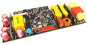
GaN Systems, the global leader in GaN (gallium nitride) power semiconductors and ON Semiconductor, a world-leading supplier of power semiconductor ICs, today announced the availability of the world’s highest power density 300 watt AC Adapter Reference Design using GaN Systems’ 650 V, 15 A GaN E-HEMTs and multiple award-winning ON Semiconductor Controller and Driver ICs: NCP51820, NCP13992, NCP1616, and NCP4306.
This complete system reference design is highly versatile and low cost, allowing designers to easily develop and bring to market ultra-high power density adapters for various applications in HDTV power supplies, gaming notebook and console adapters as well as ultra-small power supplies for industrial and medical devices.
The kit and application note provide detailed technical information including schematic, PCB layout, and BOM (bill of material) files, and EMI and efficiency data. The kit hardware has complete PFC, LLC, and secondary stages, and features a high-efficiency synchronous PFC which meets CoC T2 benchmark, a highly-versatile low-cost 2-Layer design, and universal input with 19 V Output at 340 W peak. System designers using this GaN-based reference design can reach power densities up to 32 watts per cubic inch.
“Fast-switching GaN works effectively with our advanced controller and drivers to optimize system designs for high power density, removing design barriers and enabling designers to take advantage of the numerous benefits provided by GaN E-HEMTs,” stated Ryan Zahn, Director of Marketing at ON Semiconductor. “With rising interest and adoption of GaN, we look forward to continued collaboration with GaN Systems to support and meet the new power requirements taking place across many industries.”
“Our collaboration combines ON Semiconductors’ system applications expertise and industry-leading power IC products with the world’s most advanced 650 V GaN E-HEMTs. This reference design developed in collaboration with ON Semiconductor makes it easier and more cost effective to design as GaN gains popularity as a building block in the adapter market,” said Charles Bailley, Senior Director, Worldwide Business Development at GaN Systems. “This release is the first of several systems and integrated packaging innovations in development, which will significantly expand the GaN ecosystem.”


