-
- News
- Books
Featured Books
- smt007 Magazine
Latest Issues
Current IssueSpotlight on India
We invite you on a virtual tour of India’s thriving ecosystem, guided by the Global Electronics Association’s India office staff, who share their insights into the region’s growth and opportunities.
Supply Chain Strategies
A successful brand is built on strong customer relationships—anchored by a well-orchestrated supply chain at its core. This month, we look at how managing your supply chain directly influences customer perception.
What's Your Sweet Spot?
Are you in a niche that’s growing or shrinking? Is it time to reassess and refocus? We spotlight companies thriving by redefining or reinforcing their niche. What are their insights?
- Articles
- Columns
- Links
- Media kit
||| MENU - smt007 Magazine
SMTA Certifies Process Engineers in Thailand and Malaysia
February 10, 2020 | SMTAEstimated reading time: 1 minute

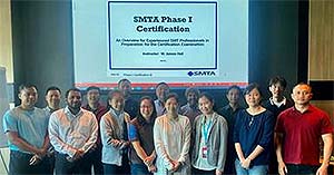
SMTA held certification programs for SMT Processes in Chonburi, Thailand, on January 14-16, 2020 and in Penang, Malaysia, on January 21-23, 2020. Over 75% of the engineers successfully passed the exams, establishing competitive credentials as "Certified" by the SMTA in SMT Processes.
The title earned by Certified SMT Process Engineers is CSMTPE. These initials, which can be added after the names of those who have passed the course, are well recognized within the industry as identifying a high level of process engineering knowledge and expertise.
The three-day program includes a day and a half of training with homework assignments, a closed book two-hour exam and an open book final exam lasting up to 6 hours. A score of 70% or greater over both exams is required to attain certification. The SMTA certification program is unique, as it recognizes and certifies the entire SMT assembly process at an engineering level.
Jim Hall, SMTA senior instructor said, “this was a great group, they were very focused and asked some extremely good questions.”
The certification is valid for five years at which point engineers have an option to be re-certified. A list of all SMTA-certified engineers is published online here:
https://www.smta.org/certification/certified_engineers.cfm
For more information, please visit https://www.smta.org/certification/ or email certification@smta.org
Testimonial
"Our marketing partnership with I-Connect007 is already delivering. Just a day after our press release went live, we received a direct inquiry about our updated products!"
Rachael Temple - AlltematedSuggested Items
Sustainability and Selective Soldering
09/15/2025 | Dr. Samuel J. McMaster, Pillarhouse InternationalSustainability is more than just a buzzword for the electronics industry; it’s a key goal for all manufacturing processes. This is more than a box-ticking exercise or simply doing a small part for environmentally friendly processes. Moving toward sustainable solutions drives innovation and operational efficiency.
Trouble in Your Tank: Implementing Direct Metallization in Advanced Substrate Packaging
09/15/2025 | Michael Carano -- Column: Trouble in Your TankDirect metallization systems based on conductive graphite are gaining popularity throughout the world. The environmental and productivity gains achievable with this process are outstanding. Direct metallization reduces the costs of compliance, waste treatment, and legal issues related to chemical exposure. A graphite-based direct plate system has been devised to address these needs.
EV Group Achieves Breakthrough in Hybrid Bonding Overlay Control for Chiplet Integration
09/12/2025 | EV GroupEV Group (EVG), a leading provider of innovative process solutions and expertise serving leading-edge and future semiconductor designs and chip integration schemes, today unveiled the EVG®40 D2W—the first dedicated die-to-wafer overlay metrology platform to deliver 100 percent die overlay measurement on 300-mm wafers at high precision and speeds needed for production environments. With up to 15X higher throughput than EVG’s industry benchmark EVG®40 NT2 system designed for hybrid wafer bonding metrology, the new EVG40 D2W enables chipmakers to verify die placement accuracy and take rapid corrective action, improving process control and yield in high-volume manufacturing (HVM).
Integrating Uniplate PLBCu6 With the Digital Factory Suite
09/12/2025 | Giovanni Obino and Andreas Schatz, MKS' AtotechPrinted circuit board manufacturing is rapidly changing, driven by miniaturization, stringent reliability requirements, and growing pressure for sustainable production. Meeting these challenges requires more than incremental improvements; it demands a combination of precise equipment and real-time process intelligence. The pairing of Uniplate® PLBCu6 with the Digital Factory Suite (DFS) demonstrates how hardware and software can work together to create more responsive, resource-efficient manufacturing.
Closing the Loop on PCB Etching Waste
09/09/2025 | Shawn Stone, IECAs the PCB industry continues its push toward greener, more cost-efficient operations, Sigma Engineering’s Mecer System offers a comprehensive solution to two of the industry’s most persistent pain points: etchant consumption and rinse water waste. Designed as a modular, fully automated platform, the Mecer System regenerates spent copper etchants—both alkaline and acidic—and simultaneously recycles rinse water, transforming a traditionally linear chemical process into a closed-loop system.