


 It’s Only Common Sense: Selling to Today's Generation of Buyers
 Dan’s Biz Bookshelf: ‘Believe in Better'
 The Big Picture: Our Big ‘Why’ in the Age of AI


Estimated reading time: 5 minutes

Language of Electronics: Transitioning From Contact Exposure to DI Solder Mask
Introduction
In the first of the commentaries from Orbotech West domain experts, Raanan Novik, our PCB process and Orbotech Diamond expert, will address one of the biggest issues faced by imaging engineers in PCB manufacturing facilities: the difficulty of exposing solder mask with increasingly tighter clearances and smaller features. The intent of our series is to provide customers and others with knowledge and tips for maximizing the value of manufacturing systems. Here, Raanan discusses the key motivators for transitioning to directly imaged (DI) solder mask exposure and ways to do so successfully.
Transitioning From Contact Exposure to DI Solder Mask
by Raanan Novik
One of my first vivid memories as a process engineer on the production floor, close to 20 years ago, was the sight of a worker hunched over a green-colored panel, straining his eyes to register Diazo film artwork to a panel intended for solder mask exposure. This operator was dressed head-to-toe in cleanroom attire, illuminated by dull-yellow lighting with the smell of solvent fumes in the air, trying to fit the pads on the film to their counterparts on the boards. Once he was successful in one area of the board, he would quickly tape the film down and move to the next corner, sometimes raising his hands in frustration when the image just wouldn’t fit. This was around the turn of the millennium, when lines and pads were still quite “robust,” to put it mildly.
Later on, I came to the realization that there exists a class of registration maestros: those that could see “the matrix” while sitting at the light table and register the toughest of board designs by manipulating the film in various fashions; measuring the temperature, humidity, and wind speed in the cleanroom to the fourth decimal place; and sometimes even artfully cutting the artwork into a puzzle of workable pieces. But even these maestros broke down sometimes when the film just wouldn’t do as it was told, and the film department would need to put it through endless iterations to find the right scale and warpage correcting factors to image the solder mask of each individual panel in the batch.
These frustrating, eye-straining jobs became more and more common in the solder mask department as laser direct imaging (LDI) and laser drilling were embraced by the pattern fabrication departments. These advanced manufacturing technologies, along with their inherent advantages, necessitated additional and more rigorous image differentiations between panels within the same batch.
Several infamous jobs were reserved for the film registration expert or for a pair of young eyes, delaying the jobs’ advancement through solder mask imaging. This would occur towards the end of the fabrication process when all the allocated time-buffer had already been exploited in previous steps, and the customer was demanding that the product be shipped out. Advanced contact exposure machines with pin registration or automatic (motor-controlled) registration were able to handle some of the load, but the jobs considered “tough to register” still required a pair of skilled hands joined to a pair of good eyes to pass solder mask inspection.
Attempts to use LDI equipment, designed to expose photoresist, with standard LPISM (liquid photo imageable solder mask), mostly resulted in what today would be considered to be average image quality with impractically long exposure times due to the spectral incompatibility with the UV absorbance of the solder mask material. Not to mention that, in most cases, the dirtier solder mask department was detached from the very clean pattern imaging department, creating a logistical problem of schlepping unexposed solder mask panels through the corridors of the PCB shop into the cleanroom of the patterning department and then all the way back again. As a result, even if the use of LDI exposure did manage to achieve a proper image, the panels would usually be scrapped due to this back-and-forth trip.
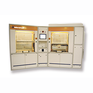
Fast forward 13 years to the PCB shop where I worked, and we received an offer to test a new direct imaging exposure machine designed specifically for solder mask. This DI machine was equipped with high-power light sources with a broad spectral output to match the exposure requirements of the solder mask we were using. Soon, we were relying on the new DI equipment for the bulk of our work in the solder mask department, allowing us to achieve superior registration with any operator and a significant reduction in reworked panels.
When I moved to my current role at Orbotech West as a process expert and a member of the company’s “experts team,” I began visiting numerous board manufacturers from California to Moscow. Repeatedly, I noted that the biggest issue faced by imaging engineers in these facilities was the difficulty to expose solder mask with increasingly tighter clearances and smaller features. All of the engineers were very interested and mostly up to date on the latest “DI for solder mask” solutions, and it was clear that there were several key motivators for transitioning to DI for solder mask exposure.
Improved solder mask registration is the most common and understandable reason to transition to DI. The solder mask image must overcome all the accumulated dimensional changes from the previous process steps, particularly when using DI for outer-layer imaging so that each panel has an individual scale. Building boards with mixed materials exacerbates the registration problem. Using film artwork isn’t cutting it anymore (excuse the pun!), leading to frequent panel rework and film re-printing, which is time-consuming and reduces yields.
From a process compatibility point of view, it is extremely beneficial to the manufacturer that, in most cases, no major pre- or post-exposure changes are required. Ink application, drying, developing, and curing parameters are rarely adjusted. The same solder mask inks may be used due to the equipment’s compatible UV-spectral output. In recent years, solder mask ink suppliers have also developed or modified products that react faster to the typical exposure spectrum of DI systems and have more efficient depth polymerization. These DI inks allow the retention of smaller features and improved sidewall quality, in addition to making exposure time with DI systems on par with that of standard contact exposure.
The financial incentives are also a big motivator for manufacturers, especially when considering the elimination of film printing and all the related equipment and operating costs of such an operation. In many shops, the solder mask department remains the sole client for film production. The reduced need for experienced and highly trained operators that can register with film is another major financial and operational advantage. In today’s climate, where unemployment rates are low, many manufacturers I visit are struggling with high employee turnover and limited labor supply. Most DI equipment, including Orbotech’s, is operated using a modest computer application, which is mastered within a couple of days and can be integrated with automation.
In summary, it is evident that direct imaging equipment for solder mask fulfills the critical demands of solder mask imaging that today’s manufacturers are facing to successfully produce their products with higher yields and at lower costs.
Share on:


