-
- News
- Books
Featured Books
- pcb007 Magazine
Latest Issues
Current IssueVoices of the Industry
We take the pulse of the PCB industry by sharing insights from leading fabricators and suppliers in this month's issue. We've gathered their thoughts on the new U.S. administration, spending, the war in Ukraine, and their most pressing needs. It’s an eye-opening and enlightening look behind the curtain.
The Essential Guide to Surface Finishes
We go back to basics this month with a recount of a little history, and look forward to addressing the many challenges that high density, high frequency, adhesion, SI, and corrosion concerns for harsh environments bring to the fore. We compare and contrast surface finishes by type and application, take a hard look at the many iterations of gold plating, and address palladium as a surface finish.
It's Show Time!
In this month’s issue of PCB007 Magazine we reimagine the possibilities featuring stories all about IPC APEX EXPO 2025—covering what to look forward to, and what you don’t want to miss.
- Articles
- Columns
Search Console
- Links
- Media kit
||| MENU - pcb007 Magazine
Elsyca Introduces New Simulation Tools for PCB Copper Balancing
April 6, 2020 | ElsycaEstimated reading time: 1 minute

Copper plating is a very complex process that is impacted by the PCB design itself, by the panel layout and by the production configuration.
The ever-increasing complexity of the design and request to deliver in shorter amounts of time are even pushing experts to—and over—their limits.
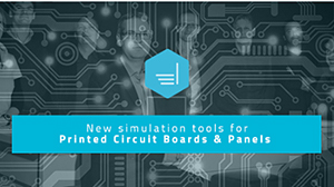
In order to support the different players in this process, Elsyca has developed a new product suite for the PCB industry. One of the products, Elsyca PCBBalance will not only provide detailed information on the layer thickness distribution, but also optimizes PCB designs/panels for manufacturing through intelligent copper balancing.
In regard to copper balancing and its importance, Rick Hartley, Principal Engineer of RHartley Enterprises commented, “Copper balancing should be done, not only at the panel level in PCB FAB, but every PCB designer should be taught the many benefits of copper balancing and incorporate the concepts into their board designs.”
Elsyca’s PCBBalance simulation software allows users to master quality by providing detailed feedback on the layer thickness distribution and on top of that, also by generating the most performant copper balancing with a single mouse click.
The most critical areas on the panel will be identified, focusing testing resources on where they are most needed.
Key features include:
- DFM
- Identify layer thickness distribution over boards and panels
- Automated and optimized copper balancing
- Identify the most critical holes for post-production quality testing
- Compare different PCB design and panel layouts side by side
- Download copper balancing results
Click on the appropriate link below to find out how this software will help you in your specific role as a PCB Designer, CAM Engineer or Process Engineer.
To learn even more about Elsyca PCBBalance, download a copy of their white paper or find out in one of their webinars how simple it works.
Suggested Items
RF PCB Design Tips and Tricks
05/08/2025 | Cherie Litson, EPTAC MIT CID/CID+There are many great books, videos, and information online about designing PCBs for RF circuits. A few of my favorite RF sources are Hans Rosenberg, Stephen Chavez, and Rick Hartley, but there are many more. These PCB design engineers have a very good perspective on what it takes to take an RF design from schematic concept to PCB layout.
Trouble in Your Tank: Causes of Plating Voids, Pre-electroless Copper
05/09/2025 | Michael Carano -- Column: Trouble in Your TankIn the business of printed circuit fabrication, yield-reducing and costly defects can easily catch even the most seasoned engineers and production personnel off guard. In this month’s column, I’ll investigate copper plating voids with their genesis in the pre-plating process steps.
Elephantech: For a Greener Tomorrow
04/16/2025 | Marcy LaRont, PCB007 MagazineNobuhiko Okamoto is the global sales and marketing manager for Elephantech Inc., a Japanese startup with a vision to make electronics more sustainable. The company is developing a metal inkjet technology that can print directly on the substrate and then give it a copper thickness by plating. In this interview, he discusses this novel technology's environmental advantages, as well as its potential benefits for the PCB manufacturing and semiconductor packaging segments.
Trouble in Your Tank: Organic Addition Agents in Electrolytic Copper Plating
04/15/2025 | Michael Carano -- Column: Trouble in Your TankThere are numerous factors at play in the science of electroplating or, as most often called, electrolytic plating. One critical element is the use of organic addition agents and their role in copper plating. The function and use of these chemical compounds will be explored in more detail.
IDTechEx Highlights Recyclable Materials for PCBs
04/10/2025 | IDTechExConventional printed circuit board (PCB) manufacturing is wasteful, harmful to the environment and energy intensive. This can be mitigated by the implementation of new recyclable materials and technologies, which have the potential to revolutionize electronics manufacturing.