


 Dan’s Biz Bookshelf: ‘The Next RenAIssance: AI and the Expansion of Human Potential’
 The Chemical Connection: When the Industry Moves Faster Than the Standards
 Driving Innovation: Selecting the Right Laser Source


Price Circuits LLC, a Division of Circuitronics, Installs LED Laser Direct Imaging System from Miva Technologies
May 12, 2020 | Price Circuits LLCEstimated reading time: 1 minute
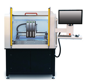
Price Circuits LLC of Elgin, IL, a leader in electronics manufacturing of printed circuit boards specializing in leading edge technologies, announces the most recent capital investment to support fine line imaging and advanced HDI products with a MIVA 2025L Di Trio Laser Direct Imaging System. Final equipment installation and training was implemented February 2020.
With our focus on supporting complex printed circuit board technologies, in rigid, flex and rigid-flex technologies, our technical capability has expanded in 2020. With technologies advancing quickly in the business industries that require the most leading edge support, Price Circuits recognized the need to update with installing the most state of the art equipment available in the industry.
The Miva LED Direct Imager is the first of its kind with precision optics, HD DMM and a custom designed LED Array to deliver a digitally defined, high UV power image to photo-sensitive substrates.
Using LDI to create the circuit traces gives us a lot of advantages, most of them pertaining to weaknesses of using a Photo-tool. Eliminating the need of a phototool removes alignment issues, light refraction issues, and those imperfections related to environmental variations. Fine lines, traces and spaces down to at least 2 mils and below are possible. It is a flexible and precise registration for various product types and variety of materials.
Price Circuits LLC has implemented over $6 million in 2019/2020 to our capital investment to better serve our diverse customer base with process capabilities to further support their ever-advancing technology needs. Our customers are coming up with demanding technologies beyond imagination and we as a company are better prepared to support their needs through the expansion.
Share on:


Subscribe
Stay ahead of the technologies shaping the future of electronics with our latest newsletter, Advanced Electronics Packaging Digest. Get expert insights on advanced packaging, materials, and system-level innovation, delivered straight to your inbox.Subscribe now to stay informed, competitive, and connected.
Suggested Items
KLA Reports Fiscal 2026 Q3 Results
04/30/2026 | PRNewswireKLA Corporation announced financial and operating results for its third quarter of fiscal year 2026, which ended on March 31, 2026, and reported GAAP net income of $1.20 billion and GAAP net income per diluted share of $9.12 on revenues of $3.415 billion.
Zhen Ding, Tsinghua University Launch Phase II R&D and Digital Transformation Program
04/30/2026 | Zhen DingZhen Ding Technology Holding Limited, a global leader in the PCB industry, held the launch ceremony for the Phase II (2026-2030) Industry-Academia Collaboration Program of the Zhen Ding-Tsinghua Joint Research Center at the Zhen Ding Technology Lecture Hall on the Tsinghua University campus.
TPCA and Industry Leaders Convene in Bangkok for Thailand PCB Summit
04/30/2026 | TPCAAt a critical juncture of global supply chain restructuring and the explosive growth in demand for AI computing power, Thailand is becoming a crucial hub for the next wave of high-end manufacturing in the electronics and circuit industry.
Jiva Soluboard Getting the Attention It Deserves
04/30/2026 | Marcy LaRont, I-Connect007 MagazineJiva is a newer company that bridges the divide between PCB fabrication and product circularity or sustainability. Jiva Soluboard is the first fully recyclable laminate material ever created for PCB fabrication, and it's not going unnoticed. Stephen Driver, CEO of Jiva, gave us an update at APEX EXPO, including an exciting certification achievement in February.
OKI Develops 180-Layer, 15 mm PCB for AI Semiconductor Test Equipment
04/29/2026 | BUSINESS WIREOKI Circuit Technology, the OKI Group’s printed circuit board (PCB) business company, has successfully developed design and production technologies for 180-layer, 15 mm-thick PCBs intended for use in wafer testing equipment for high bandwidth memory (HBM) mounted on AI semiconductors.