


 Standard of Excellence: The Future of Fabrication—From Art to Automation
 Knocking Down the Bone Pile: The Business Case for Component Reclamation
 Global Sourcing Spotlight: The Hidden Power of the Rep Network


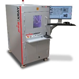
PDR X-ray Solutions is pleased to announce that its 2D and 2D+ X-ray systems have set a new industry standard for high-quality X-ray images at an affordable price. Choosing the correct system for your requirements such as X-ray for quality control or X-ray for process control is vital for the success of both X-ray circuit board inspection programs as well as X-ray semiconductor inspection programs.
PDR’s 90kV X-ray and 130kV X-ray systems are engineered with high-quality materials and craftsmanship and X-ray safety standards exceeding the most stringent requirements for industrial safety. All X-ray non-destructive inspection systems built by PDR are equipped with a suite of X-ray image processing tools and features that incorporate cutting-edge technologies to ensure that your X-ray system delivers quality X-ray images and the power of analytic tools required for a successful X-ray program.
Surface mount and assembly inspection is vital for providing quality product. PDR’s BGA X-ray defect detection and BGA X-ray inspection starts with high quality X-ray images with outstanding image clarity. This makes possible the highest level of analytical tool outcomes utilizing PDR’s proprietary software to perform a high level analysis of BGA packages, X-ray for solder ball sphere void percentage calculations, solder ball area and roundness (spherocity), as well as analytical tools to address X-ray for QFN package inspection, X-ray for CSP package inspection, and X-ray for flip chip inspection as well as X-ray for QFP package inspection and more…
PDR X-ray systems oblique view capability (up to 70°) offers the ability to rotate your sample (PCB, component, SMT device, etc.) to allow X-ray inspection of bond wire quality and perform X-ray bond wire sweep analytics, X-ray of solder fill for PTH – X-ray barrel fill analysis and more.
Whether your X-ray needs are failure analysis to detect and measure die attach voiding, bond wire Attach, etc.) only, or to resolve production issues such as X-ray solder bridging, shorts, opens, insufficient solder, solder paste inspection, head-in-pillow (HiP) issues or solder wetting issues, or simply to validate processes for X-ray inspection of array packages such as BGAs, QFNs, CSP and flip chips, PDR X-ray systems provide the tools to successfully manage your X-ray program with affordability in mind.
PDR systems are made in the USA with worldwide service and support, and one-year or multi-year warranties. PDR can help to determine the best X-ray source and detector depending on the application.


