


 The Marketing Minute: If Your Marketing Budget Gets Cut in Half, Then What?
 Punching Out: How Are the Big Boys in Electronics Doing?
 It’s Only Common Sense: Complexity Is the Enemy of Profit


PV Nano Cell Launches New General-Purpose Gold Ink for Digital Conductive Printing
July 1, 2020 | Globe NewswireEstimated reading time: 2 minutes
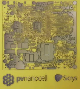
PV Nano Cell Ltd, an innovative provider of inkjet-based conductive digital printing solutions and producer of conductive digital inks, announced that it has launched a new, general-purpose conductive gold ink to be used with inkjet and aerosol printing.
The new gold ink was specially developed to meet requirements made by customers and covers a wide range of applications. The company expects many uses for the ink including with PCB, connectors, switch and relay contacts, soldered joints, plating and wire bonding. The current subtractive and plating technologies of gold are highly expensive and complicated to use. The new ink now enables a simple, digital, additive, mass-production technology.
This additive technology guarantees the best manufacturing cost while offering a new level of design flexibility and product time-to-market. This new commercial ink will complement the company’s existing product line of silver, copper and dielectric inks.
PV Nano Cell’s Chief Executive Officer, Dr. Fernando de la Vega, commented, “For digital printed electronics in mass production to become the mainstream, additional inks and printing solutions need to be developed to address inherent challenges. Such challenges include for example reducing corrosion, enabling soldering and wire bonding, etc. The ability to inkjet or aerosol-print our gold ink is a significant step forward to further enable digital printing to become widely used. This new product will drive new, high-performance and reliable electronics in the most competitive offering. As gold is used in virtually all advanced electronic devices, the market potential is overwhelming, particularly given the cost-performance bundle our new gold ink offers. We further plan to optimize the ink to our DemonJet Printer that is capable of printing up to 10 inks at the same time. Our end goal is for the printer to support our silver, dialectic, gold and resistor inks to allow customers to print a variety of pioneer products. Our advanced development of printed embedded passive components is now complemented by this new gold ink.“
As recently published earlier this month, the company announced that it has signed, under NDA, an agreement with a well-known, world-leading multinational healthcare company to develop a new inkjet printing technology for the fabrication of sensors using resistor and gold inks. This new general-purpose gold ink, differs in performance and optimization from the ink developed for healthcare applications.
PV Nano Cell’s Chief of Business Development Officer, Mr. Hanan Markovich commented, “We are being contacted frequently by customers actively looking for high-performance gold ink. Having discussed customers’ needs, we learned the market requires gold ink to address significant manufacturing issues. We further realized, current technologies and alternatives are highly expensive, inefficient and hard to implement, suggesting a great business potential. The new gold ink developed by PV Nano Cell solves real problems for customers, in an affordable way. We are now finalizing the preliminary orders and working on expanding the pipeline.“
Share on:


Testimonial
"In a year when every marketing dollar mattered, I chose to keep I-Connect007 in our 2025 plan. Their commitment to high-quality, insightful content aligns with Koh Young’s values and helps readers navigate a changing industry. "
Brent Fischthal - Koh YoungSuggested Items
I-Connect007 Releases The Printed Circuit Designer’s Guide to… Direct Metallization: A Guide to Complex PCB Fabrication
05/13/2026 | I-Connect007As PCB complexity continues to accelerate, fabricators and OEMs are reevaluating long-standing manufacturing processes to meet the demands of AI, HDI, advanced packaging, and next-generation electronics. To address these evolving challenges, I-Connect007 is proud to announce the release of The Printed Circuit Designer’s Guide to… Direct Metallization: A Guide to Complex PCB Fabrication, authored by MacDermid Alpha Solution’s Carmichael Gugliotti.
Driving Innovation: Selecting the Right Laser Source
04/28/2026 | Simon Khesin -- Column: Driving InnovationWhen I first joined Schmoll Maschinen, I brought experience from almost every PCB process, except for laser. As I immersed myself in laser processing, I realized why it can seem so daunting to a newcomer. The complexity arises from three intersecting factors: A vast variety of laser sources: CO2, UV-nano, green-pico, UV-pico, IR-pico, and others; a diverse range of applications: Drilling, cutting, ablation, and more; and an extensive list of materials: These have vastly different absorption rates. Choosing the right machine or laser source is rarely trivial. Even for experienced engineers, answering "Which source is best?" requires examining the business's specific goals.
Institute of Circuit Technology Spring Seminar 2026: A Bright Future in Europe
04/23/2026 | Pete Starkey, I-Connect007Through the leafy lanes and spring flowers of Warwickshire and back to Meridan, the traditional centre of England, and now officially part of the Metropolitan Borough of Solihull in the county of the West Midlands, I attended the Annual General Meeting and Spring Seminar of the Institute of Circuit Technology (ICT) on April 14. Out of the AGM came notable changes in leadership at the top of the Institute: the retirement of Mat Beadel as chair and Emma Hudson as technical director. Effective May 1, Steve Driver is the new chair, and Alun Morgan is the new technical director.
ACCM Unveils Negative and Near-zero CTE Materials for Large-Format AI Chips
04/21/2026 | Advanced Chip and Circuit MaterialsAdvanced Chip and Circuit Materials, Inc. (ACCM) has launched two new materials: Celeritas HM50, with a negative coefficient of thermal expansion (CTE) of -8 ppm/°C to offset the positive CTE and expansion of copper with temperature on circuit boards, and Celeritas HM001, with near-zero CTE and the low-loss performance needed for high-speed signal layers to 224 Gb/s and faster in artificial intelligence (AI) circuits.
Fresh PCB Concepts: Designing PCBs for Harsh Environments—Reliability Is Engineered Upstream
04/23/2026 | Team NCAB -- Column: Fresh PCB ConceptsWhen engineers hear the phrase “harsh environment,” they usually think of the extreme temperature swings, vibration and shock, pressure changes, or radiation in aerospace. However, aerospace is not the only harsh environment where electronic assemblies must survive. Automotive power electronics, downhole oil and gas tools, marine controls, rail systems, defense platforms, and industrial automation equipment all expose PCBs to environments that are equally unforgiving. The stress mechanisms may differ, but the physics does not.